 搜索
搜索
 发布采购
发布采购
更新日期:2024-04-01 00:04:00

产品简介:CMOS 双通道 D 类触发器
查看详情CD4013BF 供应商
- 公司
- 型号
- 品牌
- 封装/批号
- 数量
- 地区
- 日期
- 说明
- 询价
-
TI代理
-
DIP14陶瓷
23+ -
15000
-
上海市
-
-
-
中国区代理原装进口特价
-
TI代理
-
DIP14陶瓷
新批号 -
7899
-
上海市
-
-
-
原厂发货进口原装微信同步QQ893727827
-
TI
-
CDIP
23+ -
5800
-
上海市
-
-
-
进口原装现货,杜绝假货。
-
TI H
-
DIP
- -
448
-
台州
-
-
-
TI
-
PQFP
8 -
5500
-
杭州
-
-
-
原装正品现货
-
DIP
2019+ -
5800
-
上海市
-
-
-
全新原装现货
CD4013BF 中文资料属性参数
- 现有数量:0现货10,001Factory
- 价格:在售
- 系列:4000B
- 包装:管件
- 产品状态:在售
- 功能:设置(预设)和复位
- 类型:D 型
- 输出类型:补充型
- 元件数:2
- 每个元件位数:1
- 时钟频率:24 MHz
- 不同 V、最大 CL 时最大传播延迟:90ns @ 15V,50pF
- 触发器类型:正边沿
- 电流 - 输出高、低:6.8mA,6.8mA
- 电压 - 供电:3V ~ 18V
- 电流 - 静态 (Iq):20 μA
- 输入电容:5 pF
- 工作温度:-55°C ~ 125°C(TA)
- 安装类型:通孔
- 供应商器件封装:14-CDIP
- 封装/外壳:14-CDIP(0.300",7.62mm)
产品特性
- Asynchronous Set-Reset Capability
- Static Flip-Flop Operation
- Medium-Speed Operation: 16 MHz (Typical) Clock Toggle Rate at 10-V Supply
- Standardized Symmetrical Output Characteristics
- Maximum Input Current Of 1-µA at 18 V Over Full Package Temperature Range: 100 nA at 18 V and 25°C
- 100 nA at 18 V and 25°C
- Noise Margin (Over Full Package Temperature Range): 1 V at VDD = 5 V 2 V at VDD = 10 V 2.5 V at VDD = 15 V
- 1 V at VDD = 5 V
- 2 V at VDD = 10 V
- 2.5 V at VDD = 15 V
产品概述
The CD4013B device consists of two identical, independent data-type flip-flops. Each
flip-flop has independent data, set, reset, and clock inputs and Q and Q
outputs. These devices can be used for shift register applications, and, by connecting
Q output to the data input, for counter and toggle applications. The logic
level present at the D input is transferred to the Q output during the positive-going transition of
the clock pulse. Setting or resetting is independent of the clock and is accomplished by a high
level on the set or reset line, respectively.The CD4013B types are supplied in 14-pin dual-in-line plastic packages (E suffix), 14-pin
small-outline packages (M, MT, M96, and NSR suffixes), and 14-pin thin shrink small-outline packages (PW and PWR suffixes).
CD4013BF 数据手册
| 数据手册 | 说明 | 数量 | 操作 |
|---|---|---|---|
 CD4013BF3A CD4013BF3A
|
CMOS DUAL D-TYPE FLIP-FLOP |
12 Pages页,519K | 查看 |
CD4013BF 电路图
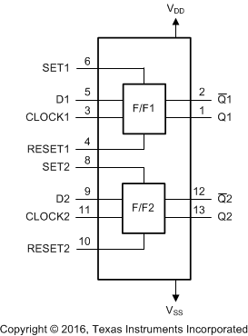
CD4013BF 电路图
CD4013BF 相关产品
- 1P1G125QDRYRQ1
- 1P1G126QDRYRQ1
- 1P2GU04QDRYRQ1
- 2N7001TDCKR
- 2N7001TDPWR
- 54FCT245TDB
- 5962-8762401CA
- 5962-8766301MRA
- 5962-8768001EA
- 7202LA50JG
- 7203L20TDB
- 7204L35J
- 72805LB15PF
- 7280L20PA
- 72V201L15PFGI
- 72V211L10PFG
- 72V245L10PFG
- 72V3640L10PF
- 72V3660L7-5PFI
- 72V70210DAG
- 72V70840DAG
- 72V73273BBG
- 74AHC05S14-13
- 74AHC05T14-13
- 74AHC1G126MDCKTEP
- 74AHC32S14-13
- 74AHC594S16-13
- 74AHC594T16-13
- 74AHCT08PW-Q100J
- 74AHCT125S14-13