 搜索
搜索
 发布采购
发布采购
更新日期:2024-04-01 00:04:00

产品简介:具有 42mW/通道功率、LVDS 接口和 CW 无源混频器的 32 通道超声波 AFE
查看详情AFE5832ZBV 供应商
- 公司
- 型号
- 品牌
- 封装/批号
- 数量
- 地区
- 日期
- 说明
- 询价
-
TI
-
原厂原装
22+ -
3288
-
上海市
-
-
-
一级代理原装
AFE5832ZBV 中文资料属性参数
- 现有数量:0现货2,100Factory
- 价格:126 : ¥2,020.07024托盘1 : ¥1,880.15000托盘
- 系列:-
- 包装:托盘托盘
- 产品状态:在售
- 位数:12
- 通道数:32
- 功率 (W):42 mW
- 电压 - 供电,模拟:3V ~ 3.3V
- 电压 - 供电,数字:3V ~ 3.3V
- 安装类型:表面贴装型
- 封装/外壳:289-FBGA
- 供应商器件封装:289-NFBGA(15x15)
产品特性
- 32-Channel, AFE for Ultrasound Applications: Input Attenuator, LNA, LPF, ADC, and CW Mixer Digital Time Gain Compensation (DTGC)Total Gain Range: 12 dB to 51 dB Linear Input Range: 800 mVPP
- Input Attenuator, LNA, LPF, ADC, and CW Mixer
- Digital Time Gain Compensation (DTGC)
- Total Gain Range: 12 dB to 51 dB
- Linear Input Range: 800 mVPP
- Input Attenuator With DTGC: 8-dB to 0-dB Attenuation With 0.125-dB Step Supports Matched Impedance for: 50-Ω to 800-Ω Source Impedance
- 8-dB to 0-dB Attenuation With 0.125-dB Step
- Supports Matched Impedance for: 50-Ω to 800-Ω Source Impedance
- 50-Ω to 800-Ω Source Impedance
- Low-Noise Amplifier (LNA) With DTGC: 20-dB to 51-dB Gain With 0.125-dB Step Low Input Current Noise: 1.2 pA/√Hz
- 20-dB to 51-dB Gain With 0.125-dB Step
- Low Input Current Noise: 1.2 pA/√Hz
- 3rd-Order, Linear-Phase, Low-Pass Filter (LPF): 5 MHz, 7.5 MHz, 10 MHz, and 12.5 MHz
- 5 MHz, 7.5 MHz, 10 MHz, and 12.5 MHz
- 16 ADCs Converting at 12-Bit, 80 MSPS or 10-bit, 100 MSPS: Each ADC Converts Two Sets of Inputs at Half Rate12-Bit ADC: 72-dBFS SNR 10-Bit ADC: 61-dBFS SNR
- Each ADC Converts Two Sets of Inputs at Half Rate
- 12-Bit ADC: 72-dBFS SNR
- 10-Bit ADC: 61-dBFS SNR
- Optimized for Noise and Power: 35 mW/Ch at 2.1 nV/√Hz, 40 MSPS42 mW/Ch at 1.4 nV/√Hz, 40 MSPS52 mW/Ch at 1.3 nV/√Hz, 40 MSPS60 mW/Ch in CW Mode
- 35 mW/Ch at 2.1 nV/√Hz, 40 MSPS
- 42 mW/Ch at 1.4 nV/√Hz, 40 MSPS
- 52 mW/Ch at 1.3 nV/√Hz, 40 MSPS
- 60 mW/Ch in CW Mode
- Excellent Device-to-Device Gain Matching: ±0.5 dB (Typical)
- ±0.5 dB (Typical)
- Low Harmonic Distortion: –55 dBc
- Fast and Consistent Overload Recovery
- Continuous Wave (CW) Path With: Low Close-In Phase Noise of –151 dBc/Hz at 1-kHz Frequency Offset Off 2.5-MHz Carrier Phase Resolution: λ / 16 Supports 16X CW Clock12-dB Suppression on Third and Fifth Harmonics
- Low Close-In Phase Noise of –151 dBc/Hz at 1-kHz Frequency Offset Off 2.5-MHz Carrier
- Phase Resolution: λ / 16
- Supports 16X CW Clock
- 12-dB Suppression on Third and Fifth Harmonics
- LVDS Interface With a Speed Up to 1 Gbps
- Small Package: 15-mm × 15-mm NFBGA-289
产品概述
The AFE5832 device is a highly-integrated, analog front-end solution
specifically designed for ultrasound systems where high performance, low power, and small size are
required.The AFE5832 is an integrated analog front-end (AFE) optimized for
medical ultrasound application. The device is realized through a multichip module (MCM) with three
dies: two voltage-controlled amplifier (VCA) dies and one analog-to-digital converter (ADC) die.
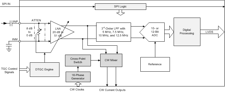
Each VCA die has 16 channels and the ADC die converts all of the 32 channels.Each channel in the VCA die is configured in either of two modes: time gain compensation
(TGC) mode or continuous wave (CW) mode. In TGC mode, each channel includes an input attenuator
(ATTEN), a low-noise amplifier (LNA) with variable-gain, and a third-order, low-pass filter (LPF).
The attenuator supports an attenuation range of 8 dB to 0 dB, and the LNA supports gain ranges from
20 dB to 51 dB. The LPF cutoff frequency can be configured at 5 MHz, 7.5 MHz, 10 MHz, or 12.5 MHz
to support ultrasound applications with different frequencies. In CW mode, each channel includes an
LNA with a fixed gain of 18 dB, and a low-power passive mixer with 16 selectable phase delays.
Different phase delays can be applied to each analog input signal to perform an on-chip beamforming
operation. A harmonic filter in the CW mixer suppresses the third and fifth harmonic to enhance the
sensitivity of the CW Doppler measurement.The ADC die has 16 physical ADCs. Each ADC converts two sets of outputs – one from each
VCA die. The ADC is configured to operate with a resolution of 12 bits or 10 bits. The ADC
resolution can be traded off with conversion rate, and operates at maximum speeds of 80 MSPS and
100 MSPS at 12-bit and 10-bit resolution, respectively. The ADC is designed to scale its power with
sampling rate. The output interface of the ADC comes out through a low-voltage differential
signaling (LVDS) which can easily interface with low-cost field-programmable gate arrays
(FPGAs).The AFE5832 also allows various power and noise combinations to be
selected for optimizing system performance. Therefore, this device is a suitable ultrasound AFE
solution for systems with strict battery-life requirements.
AFE5832ZBV 电路图
AFE5832ZBV 电路图
AFE5832ZBV 相关产品
- 5962-0720401VXC
- 5962-0720801VXC
- 5962-87802012A
- 5962-9152101MXA
- 5962-9961601HXA
- 6PA3100IRHBRQ1
- AD2S1210SST-EP-RL7
- AD2S1210WDSTZ
- AD2S80ATD/B
- AD3421QRWERQ1
- AD3421QRWETQ1
- AD5122ABCPZ100-RL7
- AD5122BCPZ100-RL7
- AD5122BRUZ10
- AD5123BCPZ100-RL7
- AD5142BCPZ10-RL7
- AD5235BRU25-EP-RL7
- AD5317RBRUZ
- AD5317RBRUZ-RL7
- AD5372BCPZ
- AD5623RBCPZ-5REEL7
- AD5628BCBZ-1-RL7
- AD5668BCPZ-1500RL7
- AD5684ARUZ
- AD5684BCPZ-RL7
- AD5684BRUZ-RL7
- AD5686ACPZ-RL7
- AD5686ARUZ
- AD5686BRUZ
- AD5686BRUZ-RL7