 搜索
搜索
 发布采购
发布采购
- 封装:64-VFQFN 裸露焊盘
- RoHS:无铅 / 符合限制有害物质指令(RoHS)规范要求
- 包装方式:带卷 (TR)
- 参考价格:$38.93
更新日期:2024-04-01 00:04:00

产品简介:四通道、12 位、65MSPS 模数转换器 (ADC)
查看详情- 封装:64-VFQFN 裸露焊盘
- RoHS:无铅 / 符合限制有害物质指令(RoHS)规范要求
- 包装方式:带卷 (TR)
- 参考价格:$38.93
ADS6422IRGCR 供应商
- 公司
- 型号
- 品牌
- 封装/批号
- 数量
- 地区
- 日期
- 说明
- 询价
-
TI
-
原厂原装
22+ -
3288
-
上海市
-
-
-
一级代理原装
-
TI(德州仪器)
-
VQFN-64(9x9)
2022+ -
12000
-
上海市
-
-
-
原装可开发票
ADS6422IRGCR 中文资料属性参数
- 产品培训模块:Data Converter Basics
- 标准包装:2,000
- 类别:集成电路 (IC)
- 家庭:数据采集 - 模数转换器
- 系列:-
- 位数:12
- 采样率(每秒):65M
- 数据接口:LVDS,并联,串行
- 转换器数目:4
- 功率耗散(最大):-
- 电压电源:模拟和数字
- 工作温度:-40°C ~ 85°C
- 安装类型:表面贴装
- 封装/外壳:64-VFQFN 裸露焊盘
- 供应商设备封装:64-VQFN 裸露焊盘(9x9)
- 包装:带卷 (TR)
- 输入数目和类型:4 个差分,单极
- 配用:296-30689-ND - EVAL MODULE FOR ADS6422
产品特性
- 12-Bit Resolution With No Missing Codes
- Simultaneous Sample and Hold
- 3.5dB Coarse Gain and upto 6dB Programmable Fine Gain for SFDR/SNR Trade-Off
- Serialized LVDS Outputs With Programmable Internal Termination Option
- Supports Sine, LVCMOS, LVPECL, LVDS Clock Inputs and Amplitude down to 400 mVPP
- Internal Reference With External Reference Support
- No External Decoupling Required for References
- 3.3-V Analog and Digital Supply
- 64 QFN Package (9 mm × 9 mm)
- Pin Compatible 14-Bit Family (ADS644X - SLAS531A)
- Feature Compatible Dual Channel Family (ADS624X - SLAS542A, ADS622X - SLAS543A)
产品概述
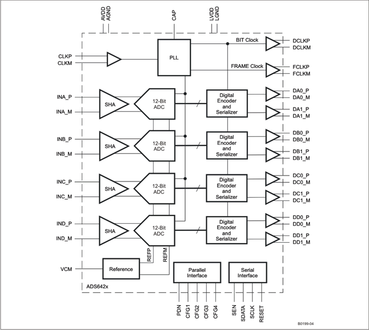
The ADS6424/ADS6423/ADS6422 (ADS642X) is a family of high performance 12-bit 105/80/65
MSPS quad channel A-D converters. Serial LVDS data outputs reduce the number of interface lines,
resulting in a compact 64-pin QFN package (9 mm × 9 mm) that allows for high system integration
density. The device includes 3.5dB coarse gain option that can be used to improve SFDR performance
with little degradation in SNR. In addition to the coarse gain, fine gain options also exist,
programmable in 1dB steps up to 6dB.The output interface is 2-wire, where each ADC data is serialized and output over two
LVDS pairs. This makes it possible to halve the serial data rate (compared to a 1-wire interface)
and restrict it to less than 1Gbps easing receiver design. The ADS642X also includes the
traditional 1-wire interface that can be used at lower sampling frequencies.An internal phase lock loop (PLL) multiplies the incoming ADC sampling clock to derive
the bit clock. The bit clock is used to serialize the 12-bit data from each channel. In addition to
the serial data streams, the frame and bit clocks are also transmitted as LVDS outputs. The LVDS
output buffers have features such as programmable LVDS currents, current doubling modes and
internal termination options. These can be used to widen eye-openings and improve signal integrity,
easing capture by the receiver.The ADC channel outputs can be transmitted either as MSB or LSB first and 2s complement
or straight binary.ADS642X has internal references, but can also support an external reference mode. The
device is specified over the industrial temperature range (–40°C to 85°C).
ADS6422IRGCR 电路图
ADS6422IRGCR 电路图
ADS6422IRGCR 相关产品
- 6PADC3101TRGERQ1
- AD1674ARZ
- AD1674BRZ
- AD1674JNZ
- AD1674KRZ
- AD1974YSTZ
- AD5590BBCZ
- AD573KNZ
- AD574AJPZ
- AD574AKE
- AD574AKP
- AD574ALD
- AD574ALNZ
- AD6600ASTZ
- AD6600ASTZ-REEL
- AD6644ASTZ-40
- AD6645ASVZ-80
- AD6654CBC
- AD670JP
- AD670JPZ
- AD670JPZ-REEL7
- AD670KNZ
- AD673JNZ
- AD674BARZ
- AD674BJNZ
- AD674BKNZ
- AD676JDZ
- AD676JN
- AD676JNZ
- AD677JRZ-REEL