 搜索
搜索
 发布采购
发布采购
- 封装:64-VFQFN 裸露焊盘
- RoHS:无铅 / 符合限制有害物质指令(RoHS)规范要求
- 包装方式:Digi-Reel®
- 参考价格:$58.176-$68.68
更新日期:2024-04-01 00:04:00

产品简介:双通道、11 位、125MSPS 模数转换器 (ADC)
查看详情- 封装:64-VFQFN 裸露焊盘
- RoHS:无铅 / 符合限制有害物质指令(RoHS)规范要求
- 包装方式:Digi-Reel®
- 参考价格:$58.176-$68.68
ADS62C15IRGCT 供应商
- 公司
- 型号
- 品牌
- 封装/批号
- 数量
- 地区
- 日期
- 说明
- 询价
-
TI
-
原厂原装
22+ -
3288
-
上海市
-
-
-
一级代理原装
-
ADI/亚德诺
-
LFCSP
22+ -
55188
-
上海市
-
-
-
原装可开发票
-
TI
-
标准封装
23+ -
15000
-
上海市
-
-
-
中国区代理原装进口特价
-
TI
-
VQFN64
23+ -
5800
-
上海市
-
-
-
进口原装现货,杜绝假货。
-
ADI/亚德诺
-
-
21+ -
90000
-
上海市
-
-
ADS62C15IRGCT 中文资料属性参数
- 产品培训模块:Data Converter Basics
- 标准包装:1
- 类别:集成电路 (IC)
- 家庭:数据采集 - 模数转换器
- 系列:-
- 位数:11
- 采样率(每秒):125M
- 数据接口:串行,并联
- 转换器数目:2
- 功率耗散(最大):-
- 电压电源:模拟和数字
- 工作温度:-40°C ~ 85°C
- 安装类型:表面贴装
- 封装/外壳:64-VFQFN 裸露焊盘
- 供应商设备封装:64-VQFN 裸露焊盘(9x9)
- 包装:®
- 输入数目和类型:2 个差分,单极
- 配用:ADS62C15EVM-ND - ADS62C15EVM
- 其它名称:296-23088-6
产品特性
- Maximum Sample Rate: 125 MSPS
- 11-Bit Resolution With No Missing Codes
- 82 dBc SFDR at Fin = 117 MHz
- 67 dBFS SNR at Fin = 117 MHz
- 77.5 dBFS SNR at Fin = 117 MHz, 20MHz bandwidth using technology
- 92 dB Crosstalk
- Parallel CMOS and DDR LVDS Output Options
- 3.5 dB Coarse Gain and Programmable Fine Gain up to 6 dB for SNR/SFDR Trade-Off
- Digital Processing Block With: Offset Correction Fine Gain Correction, in Steps of 0.05 dB Decimation by 2/4/8 Built-in and Custom Programmable 24-Tap Low/High/ Band Pass Filters
- Offset Correction
- Fine Gain Correction, in Steps of 0.05 dB
- Decimation by 2/4/8
- Built-in and Custom Programmable 24-Tap Low/High/ Band Pass Filters
- Supports Sine, LVPECL, LVDS and LVCMOS Clocks and Amplitude Down to 400 mVPP
- Clock Duty Cycle Stabilizer
- Internal Reference; Also Supports External Reference
- 64-QFN Package (9mm × 9mm)
产品概述
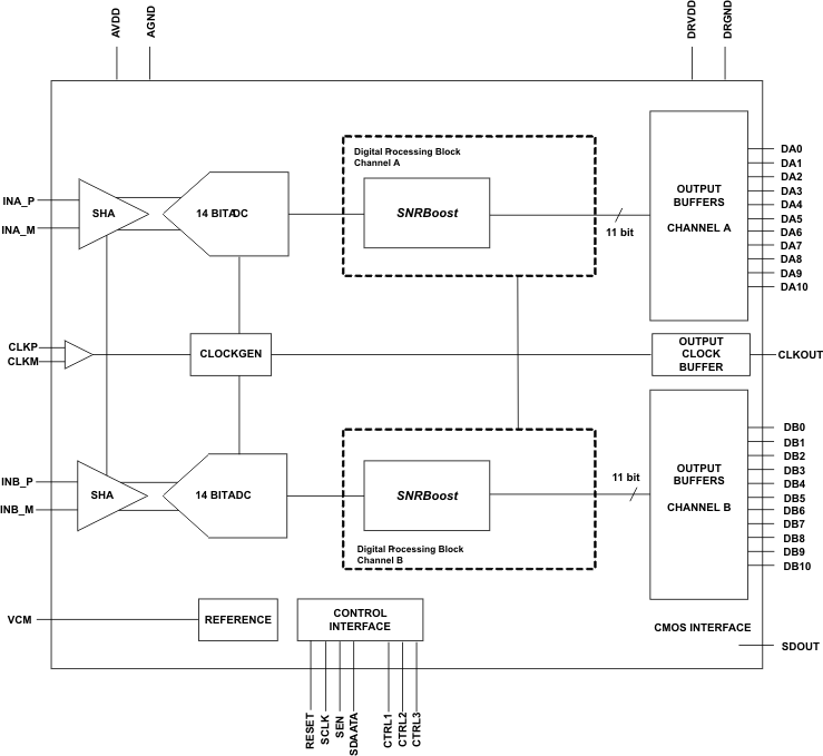
ADS62C15 is a dual channel 11-bit A/D converter with maximum sample rates up to 125 MSPS. It combines high performance and low power consumption in a compact 64 QFN package. Using an internal sample and hold and low jitter clock buffer, the ADC supports high SNR and high SFDR at high input frequencies. It has coarse and fine gain options that can be used to improve SFDR performance at lower full-scale input ranges.ADS62C15 uses proprietary technology that can be used to overcome SNR limitation due to quantization noise (for bandwidths less than Nyquist, Fs/2). It includes a digital processing block that consists of several useful and commonly used digital functions such as ADC offset correction, fine gain correction (in steps of 0.05 dB), decimation by 2,4,8 and in-built and custom programmable filters. By default, the digital processing block is bypassed, and its functions are disabled.Two output interface options exist – parallel CMOS and DDR LVDS (Double Data Rate). ADS62C15 includes internal references while traditional reference pins and associated decoupling capacitors have been eliminated. The device can also be driven with an external reference. The device is specified over the industrial temperature range (–40°C to 85°C).
ADS62C15IRGCT 数据手册
| 数据手册 | 说明 | 数量 | 操作 |
|---|---|---|---|
 ADS62C15IRGCT ADS62C15IRGCT
|
11 Bit Analog to Digital Converter 2 Input 2 Pipelined 64-VQFN (9x9) |
65页,1.58M | 查看 |
ADS62C15IRGCT 电路图
ADS62C15IRGCT 电路图
ADS62C15IRGCT 相关产品
- 6PADC3101TRGERQ1
- AD1674ARZ
- AD1674BRZ
- AD1674JNZ
- AD1674KRZ
- AD1974YSTZ
- AD5590BBCZ
- AD573KNZ
- AD574AJPZ
- AD574AKE
- AD574AKP
- AD574ALD
- AD574ALNZ
- AD6600ASTZ
- AD6600ASTZ-REEL
- AD6644ASTZ-40
- AD6645ASVZ-80
- AD6654CBC
- AD670JP
- AD670JPZ
- AD670JPZ-REEL7
- AD670KNZ
- AD673JNZ
- AD674BARZ
- AD674BJNZ
- AD674BKNZ
- AD676JDZ
- AD676JN
- AD676JNZ
- AD677JRZ-REEL