 搜索
搜索
 发布采购
发布采购
- 封装:32-VFQFN 裸露焊盘
- RoHS:无铅 / 符合限制有害物质指令(RoHS)规范要求
- 包装方式:Digi-Reel®
- 参考价格:$29.34-$37.08
更新日期:2024-04-01 00:04:00

产品简介:12 位、80MSPS 模数转换器 (ADC)
查看详情- 封装:32-VFQFN 裸露焊盘
- RoHS:无铅 / 符合限制有害物质指令(RoHS)规范要求
- 包装方式:Digi-Reel®
- 参考价格:$29.34-$37.08
ADS6123IRHBT 供应商
- 公司
- 型号
- 品牌
- 封装/批号
- 数量
- 地区
- 日期
- 说明
- 询价
-
TI
-
原厂原装
22+ -
3288
-
上海市
-
-
-
一级代理原装
-
BB
-
UNKNOWN
7 -
49
-
杭州
-
-
-
原装正品现货
-
TI(德州仪器)
-
VQFN-32
2022+ -
12000
-
上海市
-
-
-
原装可开发票
-
TI
-
QFN(RHB)-3
23+ -
5800
-
上海市
-
-
-
进口原装现货,杜绝假货。
ADS6123IRHBT 中文资料属性参数
- 产品培训模块:Data Converter Basics
- 标准包装:1
- 类别:集成电路 (IC)
- 家庭:数据采集 - 模数转换器
- 系列:-
- 位数:12
- 采样率(每秒):80M
- 数据接口:串行,并联
- 转换器数目:1
- 功率耗散(最大):-
- 电压电源:模拟和数字
- 工作温度:-40°C ~ 85°C
- 安装类型:表面贴装
- 封装/外壳:32-VFQFN 裸露焊盘
- 供应商设备封装:32-QFN 裸露焊盘(5x5)
- 包装:®
- 输入数目和类型:1 个差分,单极
- 配用:ADS6123EVM-ND - ADS6123EVM
- 其它名称:296-22702-6
产品特性
- Maximum Sample Rate: 125 MSPS
- 12-Bit Resolution with No Missing Codes
- 3.5 dB Coarse Gain and up to 6 dB Programmable Fine Gain for SNR/SFDR Trade-Off
- Parallel CMOS and Double Data Rate (DDR) LVDS Output Options
- Supports Sine, LVCMOS, LVPECL, LVDS Clock Inputs and Clock Amplitude Down to 400 mVPP
- Clock Duty Cycle Stabilizer
- Internal Reference with Support for External Reference
- No External Decoupling Required for References
- Programmable Output Clock Position and Drive Strength to Ease Data Capture
- 3.3 V Analog and 1.8 V to 3.3 V Digital Supply
- 32-QFN Package (5 mm × 5 mm)
- Pin Compatible 12-Bit Family (ADS612X)
- APPLICATIONS Wireless Communications InfrastructureSoftware Defined RadioPower Amplifier Linearization802.16d/eTest and Measurement InstrumentationHigh Definition VideoMedical ImagingRadar Systems
- Wireless Communications Infrastructure
- Software Defined Radio
- Power Amplifier Linearization
- 802.16d/e
- Test and Measurement Instrumentation
- High Definition Video
- Medical Imaging
- Radar Systems
产品概述
ADS6125/ADS6124/ADS6123/ADS6122 (ADS612X) is a family of 12-bit A/D converters with sampling frequencies up to 125 MSPS. It combines high performance and low power consumption in a compact 32 QFN package. Using an internal high bandwidth sample and hold and a low jitter clock buffer helps to achieve high SNR and high SFDR even at high input frequencies. It features coarse and fine gain options that are used to improve SFDR performance at lower full-scale analog input ranges.The digital data outputs are either parallel CMOS or DDR LVDS (Double Data Rate). Several features exist to ease data capture such as — controls for output clock position and output buffer drive strength, and LVDS current and internal termination programmability. The output interface type, gain, and other functions are programmed using a 3-wire serial interface. Alternatively, some of these functions are configured using dedicated parallel pins so that the device comes up in the desired state after power-up. ADS612X includes internal references, while eliminating the traditional reference pins and associated external decoupling. External reference mode is also supported.The devices are specified over the industrial temperature range (-40°C to 85°C).
ADS6123IRHBT 电路图
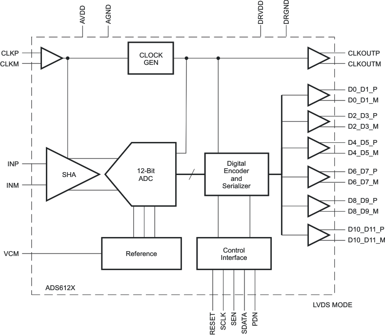
ADS6123IRHBT 电路图
ADS6123IRHBT 相关产品
- 6PADC3101TRGERQ1
- AD1674ARZ
- AD1674BRZ
- AD1674JNZ
- AD1674KRZ
- AD1974YSTZ
- AD5590BBCZ
- AD573KNZ
- AD574AJPZ
- AD574AKE
- AD574AKP
- AD574ALD
- AD574ALNZ
- AD6600ASTZ
- AD6600ASTZ-REEL
- AD6644ASTZ-40
- AD6645ASVZ-80
- AD6654CBC
- AD670JP
- AD670JPZ
- AD670JPZ-REEL7
- AD670KNZ
- AD673JNZ
- AD674BARZ
- AD674BJNZ
- AD674BKNZ
- AD676JDZ
- AD676JN
- AD676JNZ
- AD677JRZ-REEL