 搜索
搜索
 发布采购
发布采购
- 参考价格:¥660.19-¥680.34
更新日期:2024-04-01 00:04:00

ADS41B49IRGZT 供应商
- 公司
- 型号
- 品牌
- 封装/批号
- 数量
- 地区
- 日期
- 说明
- 询价
-
TI
-
原厂原装
22+ -
3288
-
上海市
-
-
-
一级代理原装
-
TI(德州仪器)
-
VQFN-48(7x7)
2022+ -
12000
-
上海市
-
-
-
原装可开发票
-
TI
-
QFN
23+ -
5800
-
上海市
-
-
-
进口原装现货,杜绝假货。
-
TI
-
TSSOP
23+ -
46000
-
合肥
-
-
-
科大讯飞战略投资企业,提供一站式配套服务
ADS41B49IRGZT 中文资料属性参数
- 制造商:Texas Instruments
- 产品种类:ADC(模数转换器)
- 转换器数量:1
- ADC 输入端数量:2
- 转换速率:250 MSPs
- 分辨率:14 bit
- 输入类型:Single-Ended, Differential
- 接口类型:Parallel
- 信噪比:69.1 dB
- Supply Voltage - Max:1.9 V
- Supply Voltage - Min:1.7 V
- 最大功率耗散:180 mW
- 最大工作温度:+ 85 C
- 安装风格:SMD/SMT
- 封装 / 箱体:QFN-48
- 封装:Reel
- 工厂包装数量:250
产品特性
- ADS41B49: 14-Bit, 250 MSPSADS41B29: 12-Bit, 250 MSPS
- Integrated High-ImpedanceAnalog Input Buffer: Input Capacitance: 2 pF 200-MHz Input Resistance: 3 kΩ
- Input Capacitance: 2 pF
- 200-MHz Input Resistance: 3 kΩ
- Maximum Sample Rate: 250 MSPS
- Ultralow Power: 1.8-V Analog Power: 180 mW 3.3-V Buffer Power: 96 mW I/O Power: 135 mW (DDR LVDS)
- 1.8-V Analog Power: 180 mW
- 3.3-V Buffer Power: 96 mW
- I/O Power: 135 mW (DDR LVDS)
- High Dynamic Performance: SNR: 69 dBFS at 170 MHz SFDR: 82.5 dBc at 170 MHz
- SNR: 69 dBFS at 170 MHz
- SFDR: 82.5 dBc at 170 MHz
- Output Interface: Double Data Rate (DDR) LVDS with Programmable Swing and Strength: Standard Swing: 350 mV Low Swing: 200 mV Default Strength: 100-Ω Termination 2x Strength: 50-Ω Termination 1.8-V Parallel CMOS Interface Also Supported
- Double Data Rate (DDR) LVDS with Programmable Swing and Strength: Standard Swing: 350 mV Low Swing: 200 mV Default Strength: 100-Ω Termination 2x Strength: 50-Ω Termination
- Standard Swing: 350 mV
- Low Swing: 200 mV
- Default Strength: 100-Ω Termination
- 2x Strength: 50-Ω Termination
- 1.8-V Parallel CMOS Interface Also Supported
- Programmable Gain for SNR, SFDR Trade-Off
- DC Offset Correction
- Supports Low Input Clock Amplitude
- Package: VQFN-48 (7 mm × 7 mm)
产品概述
The ADS41Bx9 are members of the ultralow-power ADS4xxx analog-to-digital converter (ADC) family, featuring integrated analog input buffers. These devices use innovative design techniques to achieve high dynamic performance, and consume extremely low power. The analog input pins have buffers, with benefits of constant performance and input impedance across a wide frequency range. The devices are well-suited for multi-carrier, wide bandwidth communications applications such as PA linearization.The ADS41Bx9 have features such as digital gain and offset correction. The gain option can be used to improve SFDR performance at lower full-scale input ranges, especially at high input frequencies. The integrated dc offset correction loop can be used to estimate and cancel the ADC offset. At lower sampling rates, the ADC automatically operates at scaled-down power with no loss in performance.The devices support both double data rate (DDR) low-voltage differential signaling (LVDS) and parallel CMOS digital output interfaces. The low data rate of the DDR LVDS interface (maximum 500 MBPS) makes using low-cost field-programmable gate array (FPGA)-based receivers possible. The devices have a low-swing LVDS mode that can be used to further reduce the power consumption. The strength of the LVDS output buffers can also be increased to support 50-Ω differential termination.The devices are available in a compact VQFN-48 package and are specified over the industrial temperature range (–40°C to +85°C).
ADS41B49IRGZT 数据手册
| 数据手册 | 说明 | 数量 | 操作 |
|---|---|---|---|
 ADS41B49IRGZT ADS41B49IRGZT
|
14 bit 250MSPS Buffered Low Power ADC 48-QFN -40 to 85 |
64页,1.68M | 查看 |
ADS41B49IRGZT 电路图
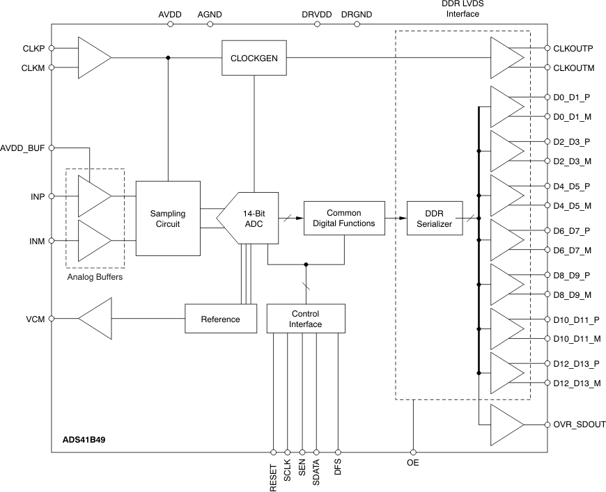
ADS41B49IRGZT 电路图
ADS41B49IRGZT 相关产品
- 100301QC
- 100304QC
- 100310QC
- 100311QC
- 100313QC
- 100316QC
- 100322QC
- 100329APC
- 100329DC
- 100336DC
- 100336PC
- 100341QC
- 100351DC
- 100351PC
- 100363QC
- 100364QC
- 100370QC
- 100390QC
- 100398QI
- 11AA010T-I/TT
- 11AA160T-I/TT
- 11LC010T-I/TT
- 11LC020T-I/TT
- 11LC040T-E/TT
- 11LC160T-E/TT
- 1ED020I12-F
- 2304NZGI-1LF
- 23A640-I/SN
- 23K256-I/SN
- 23K256-I/ST