 搜索
搜索
 发布采购
发布采购
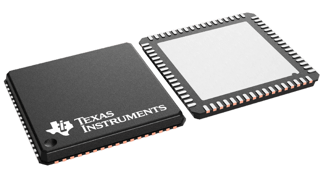
ADC16DV160CILQX/NOPB
数据转换 IC- 参考价格:¥1,030.52
更新日期:2024-04-01 00:04:00
ADC16DV160CILQX/NOPB 供应商
- 公司
- 型号
- 品牌
- 封装/批号
- 数量
- 地区
- 日期
- 说明
- 询价
-
TI(德州仪器)
-
VQFN-68
2022+ -
12000
-
上海市
-
-
-
原装可开发票
ADC16DV160CILQX/NOPB 中文资料属性参数
- 制造商:National Semiconductor (TI)
- 转换器数量:2
- ADC 输入端数量:2
- 结构:Pipelined
- 转换速率:160000 KSPs
- 分辨率:16 bit
- 输入类型:Voltage
- 接口类型:Serial (3-Wire, SPI), LVDS
- 信噪比:78.5 dB
- 电压参考:Internal, External
- Supply Voltage - Max:1.9 V, 3.6 V
- Supply Voltage - Min:1.7 V, 2.7 V
- 最大功率耗散:1300 mW
- 最大工作温度:+ 85 C
- 封装 / 箱体:LLP EP
- 封装:Reel
- 最小工作温度:- 40 C
- 工作电源电压:1.8 V, 3.3 V
- 工厂包装数量:2000
产品特性
- Low Power Consumption
- On-Chip Precision Reference and Sample-and-Hold Circuit
- On-Chip Automatic Calibration During Power-Up
- Dual Data Rate LVDS Output Port
- Dual Supplies: 1.8V and 3.0V Operation
- Selectable Input Range: 2.4 and 2.0 VPP
- Sampling Edge Flipping with Clock Divider by 2 Option
- Internal Clock Divide by 1 or 2
- On-Chip Low Jitter Duty-Cycle Stabilizer
- Power-Down and Sleep Modes
- Output Fixed Pattern Generation
- Output Clock Position Adjustment
- 3-Wire SPI
- Offset Binary or 2's Complement Data Format
- 68-Pin VQFN Package (10x10x0.8, 0.5mm Pin-Pitch)
- Resolution: 16 Bits
- Conversion Rate: 160 MSPS
- SNR (@FIN = 30 MHz): 78 dBFS (typ)
- SNR (@FIN = 197 MHz): 76 dBFS (typ)
- SFDR (@FIN = 30 MHz): 95 dBFS (typ)
- SFDR (@FIN = 197 MHz): 89 dBFS (typ)
- Full Power Bandwidth: 1.4 GHz (typ)
- Power Consumption:Core per channel: 612 mW (typ)LVDS Driver: 117 mW (typ)Total: 1.3W (typ)
- Core per channel: 612 mW (typ)
- LVDS Driver: 117 mW (typ)
- Total: 1.3W (typ)
- Operating Temperature Range (-40°C ~ 85°C)
产品概述
The ADC16DV160 is a monolithic dual channel high performance CMOS
analog-to-digital converter capable of converting analog input signals into 16-bit digital words at
rates up to 160 Mega Samples Per Second (MSPS). This converter uses a differential, pipelined
architecture with digital error correction and an on-chip sample-and-hold circuit to minimize power
consumption and external component count while providing excellent dynamic performance. Automatic
power-up calibration enables excellent dynamic performance and reduces part-to-part variation, and
the ADC16DV160 can be re-calibrated at any time through the 3-wire Serial Peripheral Interface
(SPI). An integrated low noise and stable voltage reference and differential reference buffer
amplifier eases board level design. The on-chip duty cycle stabilizer with low additive jitter
allows a wide range of input clock duty cycles without compromising dynamic performance. A unique
sample-and-hold stage yields a full-power bandwidth of 1.4 GHz. The interface between the
ADC16DV160 and a receiver block can be easily verified and optimized via fixed pattern generation
and output clock position features. The digital data is provided via dual data rate LVDS outputs –
making possible the 68-pin, 10 mm x 10 mm VQFN package. The ADC16DV160 operates on dual power
supplies of +1.8V and +3.0V with a power-down feature to reduce power consumption to very low
levels while allowing fast recovery to full operation.
ADC16DV160CILQX/NOPB 数据手册
| 数据手册 | 说明 | 数量 | 操作 |
|---|---|---|---|
 ADC16DV160CILQX/NOPB ADC16DV160CILQX/NOPB
|
16 Bit Analog to Digital Converter 2 Input 2 Pipelined 68-VQFN (10x10) |
38页,1.37M | 查看 |
ADC16DV160CILQX/NOPB 电路图
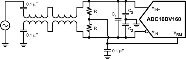
ADC16DV160CILQX/NOPB 电路图
ADC16DV160CILQX/NOPB 相关产品
- 100301QC
- 100304QC
- 100310QC
- 100311QC
- 100313QC
- 100316QC
- 100322QC
- 100329APC
- 100329DC
- 100336DC
- 100336PC
- 100341QC
- 100351DC
- 100351PC
- 100363QC
- 100364QC
- 100370QC
- 100390QC
- 100398QI
- 11AA010T-I/TT
- 11AA160T-I/TT
- 11LC010T-I/TT
- 11LC020T-I/TT
- 11LC040T-E/TT
- 11LC160T-E/TT
- 1ED020I12-F
- 2304NZGI-1LF
- 23A640-I/SN
- 23K256-I/SN
- 23K256-I/ST