 搜索
搜索
 发布采购
发布采购
更新日期:2024-04-01 00:04:00

产品简介:汽车类 14 位 200kSPS 伪差分微功耗模数转换器 (ADC)
查看详情ADC141S628QIMM/NOPB 供应商
- 公司
- 型号
- 品牌
- 封装/批号
- 数量
- 地区
- 日期
- 说明
- 询价
-
TI
-
原厂原装
22+ -
3288
-
上海市
-
-
-
一级代理原装
ADC141S628QIMM/NOPB 中文资料属性参数
- 现有数量:0现货3,000Factory查看交期
- 价格:1,000 : ¥62.96323卷带(TR)
- 系列:Automotive, AEC-Q100
- 包装:卷带(TR)
- 产品状态:在售
- 位数:14
- 采样率(每秒):200k
- 输入数:2
- 输入类型:个伪差分
- 数据接口:MICROWIRE?,QSPI?,串行,SPI?
- 配置:-
- 比率 - S/H:ADC:-
- A/D 转换器数:1
- 架构:SAR
- 参考类型:外部
- 电压 - 供电,模拟:4.5V ~ 5.5V
- 电压 - 供电,数字:4.5V ~ 5.5V
- 特性:-
- 工作温度:-40°C ~ 105°C
- 封装/外壳:10-TFSOP,10-MSOP(0.118",3.00mm 宽)
- 供应商器件封装:10-VSSOP
- 安装类型:表面贴装型
产品特性
- Qualified for Automotive Applications
- AEC-Q100 Qualified With the Following Results: Device Temperature Grade 2: –40°C to 105°C Ambient Operating Temperature Range Device HBM ESD Classification Level H2 Device CDM ESD Classification Level C6
- Device Temperature Grade 2: –40°C to 105°C Ambient Operating Temperature Range
- Device HBM ESD Classification Level H2
- Device CDM ESD Classification Level C6
- 14-Bit Resolution With no Missing Codes
- Specified Performance Up to 200 kSPS
- Pseudo Differential Inputs
- Zero-Power Track Mode
- ±150-mV Swing Around GND on Negative Input
- Separate Digital I/O and Analog Supplies
- Operating Temperature Range of –40°C to +105°C
- SPI™, QSPI™, Microwire, DSP-Compatible Serial Interface
- Conversion Rate: 50 kSPS to 200 kSPS
- INL (–15°C to +65°C): ±0.95 LSB (max)
- DNL: ±0.95 LSB (max)
- Post Calibration TUE (–15°C to +65°C): ±0.5 mV (max)
- SNR: 80 dBc (min)
- THD: –97 dBc (typ)
- ENOB: 13.0 Bits (min)
- Power Consumption: 200 kSPS, 5 V: 4.8 mW (typ)Power-Down, 5 V: 13 µW (typ)
- 200 kSPS, 5 V: 4.8 mW (typ)
- Power-Down, 5 V: 13 µW (typ)
产品概述
The ADC141S628-Q1 device is a 14-bit, 200-kSPS, pseudo-differential, analog-to-digital
converter (ADC) that is AEC-Q100 grade 2 qualified. The converter is based on a
successive-approximation register (SAR) architecture and has pseudo-differential analog inputs. The
signal path is maintained from the internal sample-and-hold circuits throughout the ADC to provide
excellent common-mode noise rejection. The ADC141S628-Q1 features a zero-power track mode where the
ADC is consuming the minimum amount of supply current while the internal sampling capacitor tracks
the applied analog input voltage.The serial data output of the ADC141S628-Q1 is straight binary and is compatible with
several standards, such as SPI, QSPI, Microwire, and many common DSP serial interfaces. The
ADC141S628-Q1 has no latency which means the conversion result is clocked out by the serial clock
input and is the result of the conversion currently in progress.The ADC141S628-Q1 can be operated with independent analog (VA) and digital input/output
(VIO) supplies. VA and VIO can range from 4.5 V to 5.5 V and can be set independent of each other.
This functionality allows a user to maximize performance and minimize power consumption. Similarly,
the ADC141S628-Q1 uses an external reference that can be varied from 1.0 V to VA allowing users to
optimize the full dynamic range of the input. The pseudo-differential input, low power consumption,
and small size make the ADC141S628-Q1 ideal for remote data acquisition applications.Operation is specified over the temperature range of –40°C to +105°C and clock rates of
0.36 MHz to 3.6 MHz. The ADC141S628-Q1 is available in a 10-lead package.
ADC141S628QIMM/NOPB 电路图
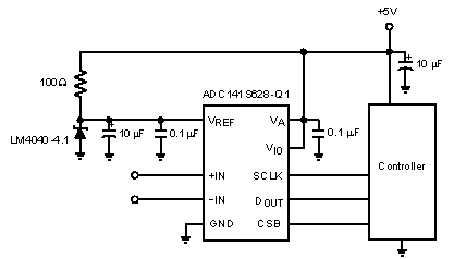
ADC141S628QIMM/NOPB 电路图
ADC141S628QIMM/NOPB 相关产品
- 5962-0720401VXC
- 5962-0720801VXC
- 5962-87802012A
- 5962-9152101MXA
- 5962-9961601HXA
- 6PA3100IRHBRQ1
- AD2S1210SST-EP-RL7
- AD2S1210WDSTZ
- AD2S80ATD/B
- AD3421QRWERQ1
- AD3421QRWETQ1
- AD5122ABCPZ100-RL7
- AD5122BCPZ100-RL7
- AD5122BRUZ10
- AD5123BCPZ100-RL7
- AD5142BCPZ10-RL7
- AD5235BRU25-EP-RL7
- AD5317RBRUZ
- AD5317RBRUZ-RL7
- AD5372BCPZ
- AD5623RBCPZ-5REEL7
- AD5628BCBZ-1-RL7
- AD5668BCPZ-1500RL7
- AD5684ARUZ
- AD5684BCPZ-RL7
- AD5684BRUZ-RL7
- AD5686ACPZ-RL7
- AD5686ARUZ
- AD5686BRUZ
- AD5686BRUZ-RL7