 搜索
搜索
 发布采购
发布采购
- 参考价格:¥285.04
更新日期:2024-04-01 00:04:00

ADC12V170CISQ 供应商
- 公司
- 型号
- 品牌
- 封装/批号
- 数量
- 地区
- 日期
- 说明
- 询价
-
National Semiconductor
-
LCC48
21+ -
419
-
上海市
-
-
-
一级代理原装
-
TI(德州仪器)
-
WQFN-48
2022+ -
12000
-
上海市
-
-
-
原装可开发票
ADC12V170CISQ 中文资料属性参数
- 制造商:National Semiconductor (TI)
- 转换器数量:1
- ADC 输入端数量:1
- 结构:Pipelined
- 转换速率:170000 KSPs
- 分辨率:12 bit
- 输入类型:Voltage
- 接口类型:Parallel, LVDS
- 信噪比:67.9 dB
- 电压参考:Internal, External
- Supply Voltage - Max:3.6 V
- Supply Voltage - Min:3 V
- 最大功率耗散:5200 mW
- 最大工作温度:+ 85 C
- 封装 / 箱体:LLP EP
- 封装:Reel
- 最小工作温度:- 40 C
- 工作电源电压:3.3 V
产品特性
- 1.1 GHz Full Power Bandwidth
- Internal Sample-and-Hold Circuit
- Internal Precision 1.0V Reference
- Single-Ended or Differential Clock Modes
- Clock Duty Cycle Stabilizer
- Dual +3.3V and +1.8V Supply Operation
- Power-Down and Sleep Modes
- Offset Binary or 2's Complement Output Data Format
- LVDS Outputs
- Pin-Compatible: ADC14V155
- 48-Pin WQFN Package, (7x7x0.8mm, 0.5mm Pin-Pitch)
- Resolution: 12 Bits
- Conversion Rate: 170 MSPS
- SNR (fIN = 70 MHz): 67.2 dBFS (Typ)
- SFDR (fIN = 70 MHz): 85.8 dBFS (Typ)
- ENOB (fIN = 70 MHz): 10.9 Bits (Typ)
- Full Power Bandwidth: 1.1 GHZ (Typ)
- Power Consumption: 781 mW (Typ)
产品概述
The ADC12V170 is a high-performance CMOS analog-to-digital converter with LVDS outputs.
It is capable of converting analog input signals into 12-Bit digital words at rates up to 170 Mega
Samples Per Second (MSPS). Data leaves the chip in a DDR (Dual Data Rate) format; this allows both
edges of the output clock to be utilized while achieving a smaller package size. This converter
uses a differential, pipelined architecture with digital error correction and an on-chip
sample-and-hold circuit to minimize power consumption and the external component count, while
providing excellent dynamic performance. A unique sample-and-hold stage yields a full-power
bandwidth of 1.1 GHz. The ADC12V170 operates from dual +3.3V and +1.8V power supplies and consumes
781 mW of power at 170 MSPS. The separate +1.8V supply for the digital output interface allows lower power operation
with reduced noise. A power-down feature reduces the power consumption to 15 mW while still
allowing fast wake-up time to full operation. In addition there is a sleep feature which consumes
50 mW of power and has a faster wake-up time. The differential inputs provide a full scale differential input swing equal to 2 times
the reference voltage. A stable 1.0V internal voltage reference is provided, or the ADC12V170 can
be operated with an external reference.Clock mode (differential versus single-ended) and output data format (offset binary
versus 2's complement) are pin-selectable. A duty cycle stabilizer maintains performance over a
wide range of input clock duty cycles.The ADC12V170 is pin-compatible with the ADC14V155. It is available in a 48-lead WQFN
package and operates over the industrial temperature range of −40°C to +85°C.
ADC12V170CISQ 数据手册
| 数据手册 | 说明 | 数量 | 操作 |
|---|---|---|---|
 ADC12V170CISQ/NOPB ADC12V170CISQ/NOPB
|
12 Bit Analog to Digital Converter 1 Input 1 Pipelined 48-WQFN (7x7) |
32页,1.13M | 查看 |
ADC12V170CISQ 电路图
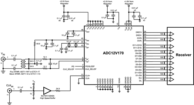
ADC12V170CISQ 电路图
ADC12V170CISQ 相关产品
- 100301QC
- 100304QC
- 100310QC
- 100311QC
- 100313QC
- 100316QC
- 100322QC
- 100329APC
- 100329DC
- 100336DC
- 100336PC
- 100341QC
- 100351DC
- 100351PC
- 100363QC
- 100364QC
- 100370QC
- 100390QC
- 100398QI
- 11AA010T-I/TT
- 11AA160T-I/TT
- 11LC010T-I/TT
- 11LC020T-I/TT
- 11LC040T-E/TT
- 11LC160T-E/TT
- 1ED020I12-F
- 2304NZGI-1LF
- 23A640-I/SN
- 23K256-I/SN
- 23K256-I/ST