 搜索
搜索
 发布采购
发布采购
- 参考价格:¥284.00
更新日期:2024-04-01 00:04:00

ADC12QS065CISQ 供应商
- 公司
- 型号
- 品牌
- 封装/批号
- 数量
- 地区
- 日期
- 说明
- 询价
-
TI
-
原厂原装
22+ -
3288
-
上海市
-
-
-
一级代理原装
-
TI(德州仪器)
-
WQFN-60
2022+ -
12000
-
上海市
-
-
-
原装可开发票
-
TI
-
原厂原封装
新批号 -
887000
-
上海市
-
-
-
原厂发货进口原装微信同步QQ893727827
ADC12QS065CISQ 中文资料属性参数
- 制造商:National Semiconductor (TI)
- 转换器数量:4
- ADC 输入端数量:4
- 结构:Pipelined
- 转换速率:65000 KSPs
- 分辨率:12 bit
- 输入类型:Voltage
- 接口类型:Serial, LVDS
- 信噪比:69.3 dB
- 电压参考:Internal, External
- Supply Voltage - Max:3.6 V
- Supply Voltage - Min:3 V
- 最大功率耗散:830 mW
- 最大工作温度:+ 85 C
- 封装 / 箱体:LLP EP
- 封装:Reel
- 最小工作温度:- 40 C
- 工作电源电压:3.3 V
- 工厂包装数量:250
产品特性
- Single +3.3V Supply Operation
- Internal Sample-and-Hold and Internal Reference
- Low Power Consumption
- Power Down Mode
- Clock and Data Frame Timing
- 780 Mbps Serial LVDS Data Rate (at 65 MHz Clock)
- LVDS Serial Output Rated for 100 Ohm Load
- Resolution: 12 Bits
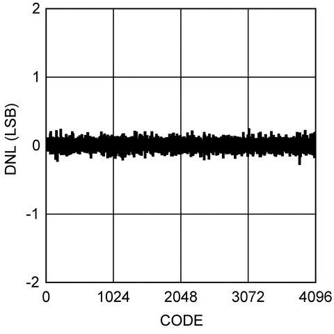
- DNL: ±0.3 LSB (Typ)
- SNR (fIN = 5 MHz): 69 dB (Typ)
- SFDR (fIN = 5 MHz): 83 dB (Typ)
- ENOB (at Nyquist): 11 Bits (Typ)
- Power ConsumptionOperating, 65 MSPS, per ADC: 200 mW (Typ)Power Down Mode: < 3 mW (Typ)
- Operating, 65 MSPS, per ADC: 200 mW (Typ)
- Power Down Mode: < 3 mW (Typ)
产品概述
The ADC12QS065 is a low power, high performance CMOS 4-channel analog-to-digital
converter with LVDS serialized outputs. The ADC12QS065 digitizes signals to 12 bits resolution at
sampling rates up to 65 MSPS while consuming a typical 200 mW/ADC from a single 3.3V supply.
Sampled data is transformed into high speed serial LVDS output data streams. Clock and frame LVDS
pairs aid in data capture. The ADC12QS065’s six differential pairs transmit data over backplanes or
cable and also make PCB design easier. In addition, the reduced cable, PCB trace count, and
connector size tremendously reduce cost. No missing codes performance is ensured over the full operating temperature range. The
pipeline ADC architecture achieves 11 Effective Bits over the entire Nyquist band at 65
MSPS.When not converting, power consumption can be reduced by pulling the PD (Power Down) pin
high, placing the converter into a low power state where it typically consumes less than 3 mW
total, and from which recovery is less than 5 ms. The ADC12QS065's speed, resolution and single
supply operation makes it well suited for a variety of applications in ultrasound, imaging, video
and communications. Operating over the industrial (-40°C to +85°C) temperature range, the
ADC12QS065 is available in a 60-pin WQFN package with exposed pad (9x9x0.8mm, 0.5mm pin pitch).
ADC12QS065CISQ 数据手册
| 数据手册 | 说明 | 数量 | 操作 |
|---|---|---|---|
 ADC12QS065CISQ/NOPB ADC12QS065CISQ/NOPB
|
12 Bit Analog to Digital Converter 4 Input 4 Pipelined 60-WQFN (9x9) |
34页,1.25M | 查看 |
ADC12QS065CISQ 电路图
ADC12QS065CISQ 电路图
ADC12QS065CISQ 相关产品
- 100301QC
- 100304QC
- 100310QC
- 100311QC
- 100313QC
- 100316QC
- 100322QC
- 100329APC
- 100329DC
- 100336DC
- 100336PC
- 100341QC
- 100351DC
- 100351PC
- 100363QC
- 100364QC
- 100370QC
- 100390QC
- 100398QI
- 11AA010T-I/TT
- 11AA160T-I/TT
- 11LC010T-I/TT
- 11LC020T-I/TT
- 11LC040T-E/TT
- 11LC160T-E/TT
- 1ED020I12-F
- 2304NZGI-1LF
- 23A640-I/SN
- 23K256-I/SN
- 23K256-I/ST