 搜索
搜索
 发布采购
发布采购
- 参考价格:¥148.83-¥150.83
更新日期:2024-04-01 00:04:00

产品简介:双通道、12 位、66MSPS、450MHz 输入带宽模数转换器 (ADC)
查看详情- 参考价格:¥148.83-¥150.83
ADC12DL066CIVS 供应商
- 公司
- 型号
- 品牌
- 封装/批号
- 数量
- 地区
- 日期
- 说明
- 询价
-
TI
-
原厂原装
22+ -
3288
-
上海市
-
-
-
一级代理原装
-
NS
-
SOP-8
23+ -
15000
-
上海市
-
-
-
中国区代理原装进口特价
-
TI
-
-
22+ -
5000
-
常州
-
-
-
全新原装现货热卖
-
NS/
-
QFP
23+ -
5800
-
上海市
-
-
-
进口原装现货,杜绝假货。
-
NS/ELNAF
-
TQFP
1835+ -
17
-
上海市
-
-
-
原装现货,精专配套,正品BOM表报价
ADC12DL066CIVS 中文资料属性参数
- 制造商:National Semiconductor (TI)
- 转换器数量:2
- ADC 输入端数量:2
- 结构:Pipelined
- 转换速率:66000 KSPs
- 分辨率:12 bit
- 输入类型:Voltage
- 接口类型:Parallel
- 信噪比:66 dB
- 电压参考:Internal, External
- Supply Voltage - Max:3.6 V
- Supply Voltage - Min:3 V
- 最大工作温度:+ 85 C
- 安装风格:SMD/SMT
- 封装 / 箱体:TQFP-64
- 封装:Tray
- 最小工作温度:- 40 C
- 工作电源电压:3.3 V
- 工厂包装数量:160
产品特性
- Choice of Binary or 2’s Complement Output Format
- Single +3.3V Supply Operation
- Outputs 2.4V to 3.3V Compatible
- Pin Compatible with ADC12D040
- Power Down Mode
- Internal/External Reference
- Resolution: 12 Bits
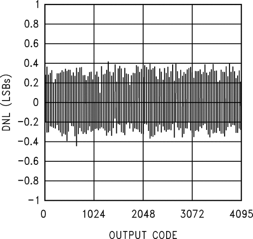
- DNL: ±0.5 LSB (typ)
- SNR (fIN = 10 MHz): 66 dB (typ)
- SFDR (fIN = 10 MHz): 81 dB (typ)
- Power ConsumptionOperating: 686 mW (typ)Power Down Mode: 75 mW (typ)
- Operating: 686 mW (typ)
- Power Down Mode: 75 mW (typ)
产品概述
The ADC12DL066 is a dual, low power monolithic CMOS analog-to-digital converter capable
of converting analog input signals into 12-bit digital words at 66 Megasamples per second (Msps),
minimum. This converter uses a differential, pipeline architecture with digital error correction
and an on-chip sample-and-hold circuit to minimize die size and power consumption while providing
excellent dynamic performance and a 450 MHz Full Power Bandwidth. Operating on a single 3.3V power
supply, the ADC12DL066 achieves 10.7 effective bits and consumes just 686 mW at 66 Msps, including
the reference current. The Power Down feature reduces power consumption to 75 mW.The differential inputs provide a full scale differential input swing equal to 2 times
VREF with the possibility of a single-ended input. Full use of the
differential input is recommended for optimum performance. The digital outputs from the two ADCs
are available on separate 12-bit buses with an output data format choice of offset binary or two’s
complement.To ease interfacing to lower voltage systems, the digital output driver power pins of the
ADC12DL066 can be connected to a separate supply voltage in the range of 2.4V to the digital supply
voltage.This device is available in the 64-lead TQFP package and will operate over the industrial
temperature range of −40°C to +85°C. An evaluation board is available to ease the evaluation
process.
ADC12DL066CIVS 数据手册
| 数据手册 | 说明 | 数量 | 操作 |
|---|---|---|---|
 ADC12DL066CIVS ADC12DL066CIVS
|
Dual 12-Bit, 66 MSPS, 450 MHz Input Bandwidth A/D Converter w/Internal Reference |
23 Pages页,655K | 查看 |
|
ADC12DL066CIVS/NOPB
|
12 Bit Analog to Digital Converter 2 Input 2 Pipelined 64-TQFP (10x10) |
33页,812K | 查看 |
ADC12DL066CIVS 电路图
ADC12DL066CIVS 电路图
ADC12DL066CIVS 相关产品
- 100301QC
- 100304QC
- 100310QC
- 100311QC
- 100313QC
- 100316QC
- 100322QC
- 100329APC
- 100329DC
- 100336DC
- 100336PC
- 100341QC
- 100351DC
- 100351PC
- 100363QC
- 100364QC
- 100370QC
- 100390QC
- 100398QI
- 11AA010T-I/TT
- 11AA160T-I/TT
- 11LC010T-I/TT
- 11LC020T-I/TT
- 11LC040T-E/TT
- 11LC160T-E/TT
- 1ED020I12-F
- 2304NZGI-1LF
- 23A640-I/SN
- 23K256-I/SN
- 23K256-I/ST