 搜索
搜索
 发布采购
发布采购
- 参考价格:¥86.87
更新日期:2024-04-01 00:04:00

ADC12DL040CIVSX 供应商
- 公司
- 型号
- 品牌
- 封装/批号
- 数量
- 地区
- 日期
- 说明
- 询价
-
TI
-
原厂原装
22+ -
3288
-
上海市
-
-
-
一级代理原装
-
TI(德州仪器)
-
64-TQFP
2022+ -
12000
-
上海市
-
-
-
原装可开发票
ADC12DL040CIVSX 中文资料属性参数
- 制造商:National Semiconductor (TI)
- 转换器数量:2
- ADC 输入端数量:2
- 结构:Pipelined
- 转换速率:40000 KSPs
- 分辨率:12 bit
- 输入类型:Voltage
- 接口类型:Parallel
- 信噪比:69 dB
- 电压参考:Internal, External
- Supply Voltage - Max:3.6 V
- Supply Voltage - Min:2.7 V
- 最大工作温度:+ 85 C
- 安装风格:SMD/SMT
- 封装 / 箱体:TQFP-64
- 封装:Reel
- 最小工作温度:- 40 C
- 工作电源电压:3 V
- 工厂包装数量:1000
产品特性
- Single +3.0V Supply Operation
- Internal Sample-and-Hold
- Internal Reference
- Outputs 2.4V to 3.6V Compatible
- Power Down Mode
- Duty Cycle Stabilizer
- Multiplexed Output Mode
- Resolution 12 Bits
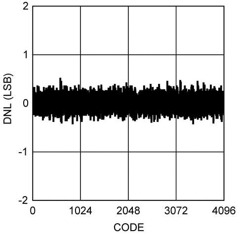
- DNL ±0.3 LSB (typ)
- SNR (fIN = 10 MHz) 69 dB (typ)
- SFDR (fIN = 10 MHz) 85 dB (typ)
- Data Latency 7 Clock Cycles
- Power ConsumptionOperating 210 mW (typ) Power Down Mode 36 mW (typ)
- Operating 210 mW (typ)
- Power Down Mode 36 mW (typ)
产品概述
The ADC12DL040 is a dual, low power monolithic CMOS analog-to-digital converter capable
of converting analog input signals into 12-bit digital words at 40 Megasamples per second (MSPS).
This converter uses a differential, pipeline architecture with digital error correction and an
on-chip sample-and-hold circuit to minimize power consumption while providing excellent dynamic
performance and a 250 MHz Full Power Bandwidth. Operating on a single +3.0V power supply, the
ADC12DL040 achieves 11.1 effective bits at nyquist and consumes just 210 mW at 40 MSPS, including
the reference current. The Power Down feature reduces power consumption to 36 mW.The differential inputs provide a full scale differential input swing equal to 2 times
VREF with the possibility of a single-ended input. Full use of the
differential input is recommended for optimum performance. The digital outputs from the two ADC's
are available on a single multiplexed 12-bit bus or on separate buses. Duty cycle stabilization and
output data format are selectable using a quad state function pin. The output data can be set for
offset binary or two's complement.To ease interfacing to lower voltage systems, the digital output driver power pins of the
ADC12DL040 can be connected to a separate supply voltage in the range of 2.4V to the analog supply
voltage.This device is available in the 64-lead TQFP package and will operate over the industrial
temperature range of −40°C to +85°C. An evaluation board is available to ease the evaluation
process.
ADC12DL040CIVSX 电路图
ADC12DL040CIVSX 电路图
ADC12DL040CIVSX 相关产品
- 100301QC
- 100304QC
- 100310QC
- 100311QC
- 100313QC
- 100316QC
- 100322QC
- 100329APC
- 100329DC
- 100336DC
- 100336PC
- 100341QC
- 100351DC
- 100351PC
- 100363QC
- 100364QC
- 100370QC
- 100390QC
- 100398QI
- 11AA010T-I/TT
- 11AA160T-I/TT
- 11LC010T-I/TT
- 11LC020T-I/TT
- 11LC040T-E/TT
- 11LC160T-E/TT
- 1ED020I12-F
- 2304NZGI-1LF
- 23A640-I/SN
- 23K256-I/SN
- 23K256-I/ST