 搜索
搜索
 发布采购
发布采购
- 参考价格:¥231.91-¥248.26
更新日期:2024-04-01 00:04:00
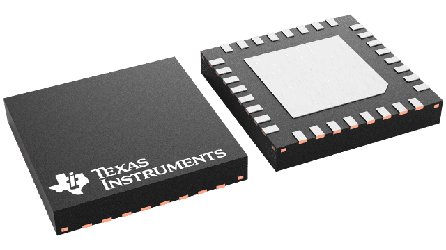
产品简介:12 位、105MSPS、1.0GHz 输入带宽模数转换器 (ADC)
查看详情- 参考价格:¥231.91-¥248.26
ADC12C105CISQE/NOPB 供应商
- 公司
- 型号
- 品牌
- 封装/批号
- 数量
- 地区
- 日期
- 说明
- 询价
-
TI
-
原厂原装
22+ -
3288
-
上海市
-
-
-
一级代理原装
-
TI(德州仪器)
-
WQFN-32(5x5)
2022+ -
12000
-
上海市
-
-
-
原装可开发票
ADC12C105CISQE/NOPB 中文资料属性参数
- 制造商:National Semiconductor (TI)
- 转换器数量:1
- ADC 输入端数量:1
- 结构:Pipelined
- 转换速率:105000 KSPs
- 分辨率:12 bit
- 输入类型:Voltage
- 接口类型:Parallel
- 信噪比:70.1 dB
- 电压参考:Internal, External
- Supply Voltage - Max:3.6 V
- Supply Voltage - Min:3 V
- 最大功率耗散:400 mW
- 最大工作温度:+ 85 C
- 封装 / 箱体:LLP EP
- 封装:Reel
- 最小工作温度:- 40 C
- 工作电源电压:3.3 V
- 工厂包装数量:250
产品特性
- 1 GHz Full Power Bandwidth
- Internal Reference and Sample-and-Hold Circuit
- Low Power Consumption
- Data Ready Output Clock
- Clock Duty Cycle Stabilizer
- Single +3.0V or +3.3V Supply Operation
- Power-Down Mode
- 32-Pin WQFN Package, (5x5x0.8mm, 0.5mm Pin-Pitch)
- Resolution: 12 Bits
- Conversion Rate: 105 MSPS
- SNR: (fIN = 240 MHz) 69 dBFS (typ)
- SFDR: (fIN = 240 MHz) 82 dBFS (typ)
- Full Power Bandwidth: 1 GHz (typ)
- Power Consumption:350 mW (typ), VA=3.0 V400 mW (typ), VA=3.3 V
- 350 mW (typ), VA=3.0 V
- 400 mW (typ), VA=3.3 V
产品概述
The ADC12C105 is a high-performance CMOS analog-to-digital converter capable of
converting analog input signals into 12-bit digital words at rates up to 105 Mega Samples Per
Second (MSPS). This converter uses a differential, pipelined architecture with digital error
correction and an on-chip sample-and-hold circuit to minimize power consumption and the external
component count, while providing excellent dynamic performance. A unique sample-and-hold stage
yields a full-power bandwidth of 1 GHz. The ADC12C105 may be operated from a single +3.0V or +3.3V
power supply and consumes low power. A separate +2.5V supply may be used for the digital output interface which allows lower
power operation with reduced noise. A power-down feature reduces the power consumption to very low
levels while still allowing fast wake-up time to full operation. The differential inputs accept a
2V full scale differential input swing. A stable 1.2V internal voltage reference is provided, or
the ADC12C105 can be operated with an external 1.2V reference. Output data format (offset binary
versus 2's complement) and duty cycle stabilizer are pin-selectable. The duty cycle stabilizer
maintains performance over a wide range of clock duty cycles.The ADC12C105 is available in a 32-lead WQFN package and operates over the industrial
temperature range of −40°C to +85°C.
ADC12C105CISQE/NOPB 数据手册
| 数据手册 | 说明 | 数量 | 操作 |
|---|---|---|---|
 ADC12C105CISQE/NOPB ADC12C105CISQE/NOPB
|
12 Bit Analog to Digital Converter 1 Input 1 Pipelined 32-WQFN (5x5) |
32页,1.27M | 查看 |
ADC12C105CISQE/NOPB 电路图
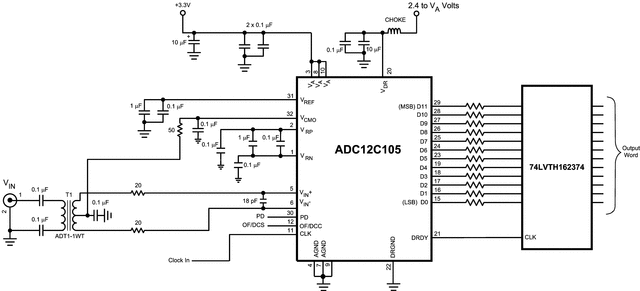
ADC12C105CISQE/NOPB 电路图
ADC12C105CISQE/NOPB 相关产品
- 100301QC
- 100304QC
- 100310QC
- 100311QC
- 100313QC
- 100316QC
- 100322QC
- 100329APC
- 100329DC
- 100336DC
- 100336PC
- 100341QC
- 100351DC
- 100351PC
- 100363QC
- 100364QC
- 100370QC
- 100390QC
- 100398QI
- 11AA010T-I/TT
- 11AA160T-I/TT
- 11LC010T-I/TT
- 11LC020T-I/TT
- 11LC040T-E/TT
- 11LC160T-E/TT
- 1ED020I12-F
- 2304NZGI-1LF
- 23A640-I/SN
- 23K256-I/SN
- 23K256-I/ST