 搜索
搜索
 发布采购
发布采购
- 参考价格:¥24.98-¥50.99
更新日期:2024-04-01 00:04:00
产品简介:双通道 12 位、200kSPS 至 500kSPS、同步采样 A/D 转换器
查看详情- 参考价格:¥24.98-¥50.99
ADC122S655CIMM/NOPB 供应商
- 公司
- 型号
- 品牌
- 封装/批号
- 数量
- 地区
- 日期
- 说明
- 询价
-
TI
-
VSSOP10
23+ -
15790
-
上海市
-
-
-
原装优势品牌
-
TI(德州仪器)
-
VSSOP-10
2022+ -
12000
-
上海市
-
-
-
原装可开发票
ADC122S655CIMM/NOPB 中文资料属性参数
- 制造商:National Semiconductor (TI)
- 转换器数量:2
- ADC 输入端数量:2
- 结构:SAR
- 转换速率:500 KSPs
- 分辨率:12 bit
- 输入类型:Voltage
- 接口类型:Serial (SPI, QSPI, Microwire)
- 信噪比:73.2 dB
- 电压参考:External
- Supply Voltage - Max:5.5 V
- Supply Voltage - Min:4.5 V
- 最大工作温度:+ 105 C
- 安装风格:SMD/SMT
- 封装 / 箱体:MSOP
- 封装:Reel
- 最小工作温度:- 40 C
- 工作电源电压:5 V
- 工厂包装数量:1000
产品特性
- True Simultaneous Sampling Differential Inputs
- Specified Performance from 200 kSPS to 500 kSPS
- External Reference
- Wide Input Common-Mode Voltage Range
- Single High-Speed Serial Data Output
- Operating Temperature Range of −40°C to +105°C
- SPI/QSPI/MICROWIRE/DSP Compatible Serial Interface
- Conversion Rate: 200 kSPS to 500 kSPS
- INL: ±1 LSB (max)
- DNL: ±0.95 LSB (max)
- SNR: 71 dBc (min)
- THD: -72 dBc (min)
- ENOB: 11.25 bits (min)
- Power Consumption at 500 kSPSConverting, VA = 5V, VREF = 2.5V: 11 mW (typ)Power-Down, VA = 5V, VREF = 2.5V: 3 µW (typ)
- Converting, VA = 5V, VREF = 2.5V: 11 mW (typ)
- Power-Down, VA = 5V, VREF = 2.5V: 3 µW (typ)
产品概述
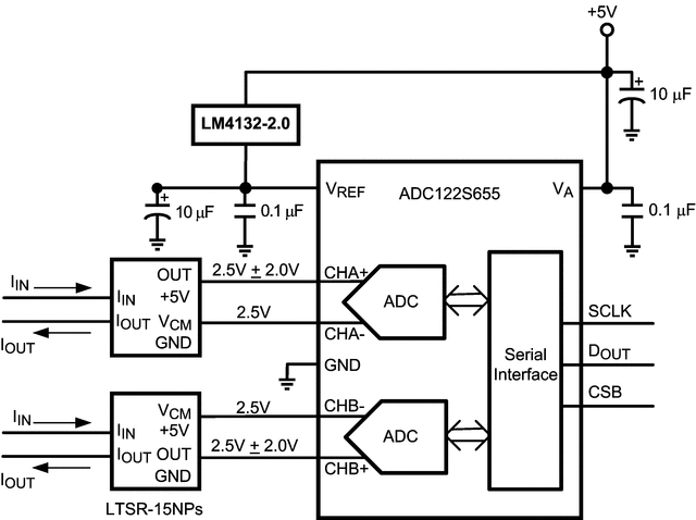
The ADC122S655 is a dual 12-bit, 200 kSPS to 500 kSPS simultaneous sampling
Analog-to-Digital (A/D) converter. The analog inputs on both channels are sampled simultaneously to
preserve their relative phase information to each other. The converter is based on a
successive-approximation register architecture where the differential nature of the analog inputs
is maintained from the internal track-and-hold circuits throughout the A/D converter to provide
excellent common-mode signal rejection. The ADC122S655 features an external reference that can be
varied from 1.0V to VA.The ADC122S655's serial data output is binary 2's complement and is compatible with
several standards, such as SPI, QSPI, MICROWIRE, and many common DSP serial interfaces. The serial
clock (SCLK) and chip select bar (CS) are shared by both channels. Operating from a single 5V analog supply and a reference voltage of 2.5V, the total power
consumption while operating at 500 kSPS is typically 11 mW. With the ADC122S655 operating in
power-down mode, the power consumption reduces to 3 µW. The differential input, low power
consumption, and small size make the ADC122S655 ideal for direct connection to sensors in motor
control applications.Operation is specified over the industrial temperature range of −40°C to +105°C and clock
rates of 6.4 MHz to 16 MHz. The ADC122S655 is available in a 10-lead VSSOP package.
ADC122S655CIMM/NOPB 电路图
ADC122S655CIMM/NOPB 电路图
ADC122S655CIMM/NOPB 相关产品
- 100301QC
- 100304QC
- 100310QC
- 100311QC
- 100313QC
- 100316QC
- 100322QC
- 100329APC
- 100329DC
- 100336DC
- 100336PC
- 100341QC
- 100351DC
- 100351PC
- 100363QC
- 100364QC
- 100370QC
- 100390QC
- 100398QI
- 11AA010T-I/TT
- 11AA160T-I/TT
- 11LC010T-I/TT
- 11LC020T-I/TT
- 11LC040T-E/TT
- 11LC160T-E/TT
- 1ED020I12-F
- 2304NZGI-1LF
- 23A640-I/SN
- 23K256-I/SN
- 23K256-I/ST