 搜索
搜索
 发布采购
发布采购
- 参考价格:¥371.63-¥399.17
更新日期:2024-04-01 00:04:00
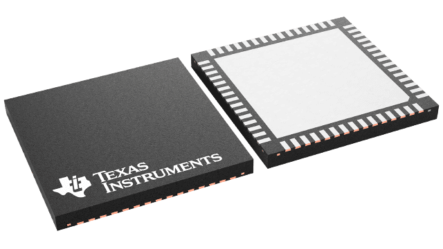
产品简介:双通道、11 位、105MSPS 模数转换器 (ADC)
查看详情- 参考价格:¥371.63-¥399.17
ADC11DS105CISQE/NOPB 供应商
- 公司
- 型号
- 品牌
- 封装/批号
- 数量
- 地区
- 日期
- 说明
- 询价
-
TI
-
原厂原装
22+ -
3288
-
上海市
-
-
-
一级代理原装
-
TI(德州仪器)
-
WQFN-60(9x9)
2022+ -
12000
-
上海市
-
-
-
原装可开发票
ADC11DS105CISQE/NOPB 中文资料属性参数
- 制造商:National Semiconductor (TI)
- 转换器数量:2
- ADC 输入端数量:2
- 结构:Pipelined
- 转换速率:105000 KSPs
- 分辨率:11 bit
- 输入类型:Voltage
- 接口类型:Serial, LVDS
- 信噪比:67.5 dB
- 电压参考:Internal, External
- Supply Voltage - Max:3.6 V
- Supply Voltage - Min:2.7 V
- 最大工作温度:+ 85 C
- 封装 / 箱体:LLP EP
- 封装:Reel
- 最小工作温度:- 40 C
- 工作电源电压:3 V, 3.3 V
- 工厂包装数量:250
产品特性
- Clock Duty Cycle Stabilizer
- Single +3.0 or +3.3V Supply Operation
- Serial LVDS Outputs
- Serial Control Interface
- Overrange Outputs
- 60-Pin WQFN Package, (9x9x0.8mm, 0.5mm Pin-Pitch)
- Resolution 11 Bits
- Conversion Rate 105 MSPS
- SNR (fIN = 240 MHz) 66 dBFS (typ)
- SFDR (fIN = 240 MHz) 82 dBFS (typ)
- Full Power Bandwidth 1 GHz (typ)
- Power Consumption 1 W (typ)
产品概述
The ADC11DS105is a high-performance CMOS analog-to-digital converters capable of
converting two analog input signals into 11-bit digital words at rates up to 105 Mega Samples Per
Second (MSPS). The digital outputs are serialized and provided on differential LVDS signal pairs.
These converters use a differential, pipelined architecture with digital error correction and an
on-chip sample-and-hold circuit to minimize power consumption and the external component count,
while providing excellent dynamic performance. The ADC11DS105 may be operated from a single +3.0 or
+3.3V power supply. A power-down feature reduces the power consumption to very low levels while
still allowing fast wake-up time to full operation. The differential inputs accept a 2V full scale
differential input swing. A stable 1.2V internal voltage reference is provided, or the ADC11DS105
can be operated with an external 1.2V reference. The selectable duty cycle stabilizer maintains
performance over a wide range of clock duty cycles. A serial interface allows access to the
internal registers for full control of the ADC11DS105's functionality. The ADC11DS105 is available
in a 60-lead WQFN package and operates over the industrial temperature range of −40°C to
+85°C.
ADC11DS105CISQE/NOPB 电路图
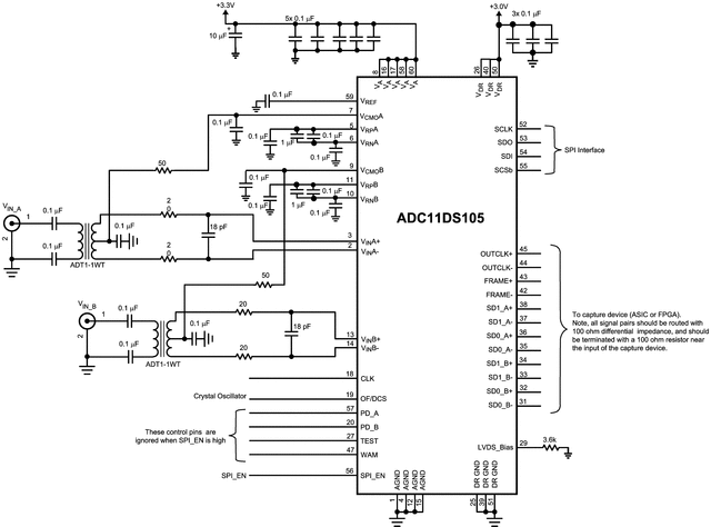
ADC11DS105CISQE/NOPB 电路图
ADC11DS105CISQE/NOPB 相关产品
- 100301QC
- 100304QC
- 100310QC
- 100311QC
- 100313QC
- 100316QC
- 100322QC
- 100329APC
- 100329DC
- 100336DC
- 100336PC
- 100341QC
- 100351DC
- 100351PC
- 100363QC
- 100364QC
- 100370QC
- 100390QC
- 100398QI
- 11AA010T-I/TT
- 11AA160T-I/TT
- 11LC010T-I/TT
- 11LC020T-I/TT
- 11LC040T-E/TT
- 11LC160T-E/TT
- 1ED020I12-F
- 2304NZGI-1LF
- 23A640-I/SN
- 23K256-I/SN
- 23K256-I/ST