 搜索
搜索
 发布采购
发布采购
- 参考价格:¥38.85-¥62.79
更新日期:2024-04-01 00:04:00
产品简介:双通道、10 位、20MSPS 模数转换器 (ADC)
查看详情- 参考价格:¥38.85-¥62.79
ADC10D020CIVS/NOPB 供应商
- 公司
- 型号
- 品牌
- 封装/批号
- 数量
- 地区
- 日期
- 说明
- 询价
-
TI
-
原厂原装
22+ -
3288
-
上海市
-
-
-
一级代理原装
ADC10D020CIVS/NOPB 中文资料属性参数
- 制造商:National Semiconductor (TI)
- 转换器数量:2
- ADC 输入端数量:2
- 结构:Pipelined
- 转换速率:20000 KSPs
- 分辨率:10 bit
- 输入类型:Voltage
- 接口类型:Parallel
- 信噪比:59 dB
- 电压参考:Internal, External
- Supply Voltage - Max:3.6 V
- Supply Voltage - Min:2.7 V
- 最大工作温度:+ 85 C
- 安装风格:SMD/SMT
- 封装 / 箱体:TQFP-48
- 封装:Tray
- 最小工作温度:- 40 C
- 工作电源电压:3 V
- 工厂包装数量:250
产品特性
- Internal Sample-and-Hold
- Internal Reference Capability
- Dual Gain Settings
- Offset Correction
- Selectable Offset Binary or 2's Complement Output
- Multiplexed or Parallel Output Bus
- Single +2.7V to 3.6V Operation
- Power Down and Standby Modes
- Resolution 10 Bits
- Conversion Rate 20 MSPS
- ENOB 9.5 Bits (typ)
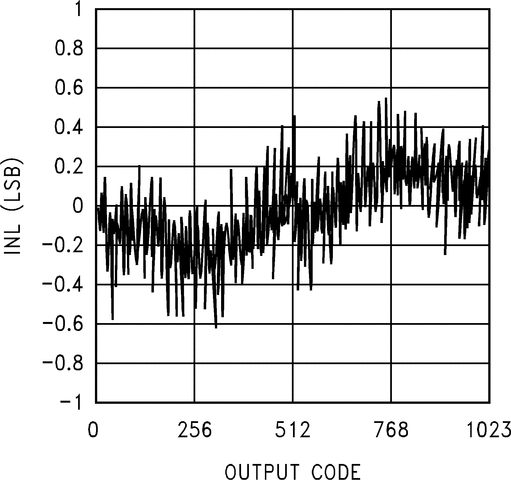
- DNL 0.35 LSB (typ)
- Conversion Latency Parallel Outputs 2.5 Clock Cycles
- Multiplexed Outputs, I Data Bus 2.5 Clock Cycles
- Multiplexed Outputs, Q Data Bus 3 Clock Cycles
- PSRR 90 dB
- Power Consumption—Normal Operation 150 mW (typ)
- Power Down Mode <1 mW (typ)
- Fast Recovery Standby Mode 27 mW (typ)
产品概述
The ADC10D020 is a dual low power, high performance CMOS analog-to-digital converter that
digitizes signals to 10 bits resolution at sampling rates up to 30 MSPS while consuming a typical
150 mW from a single 3.0V supply. No missing codes is ensured over the full operating temperature
range. The unique two stage architecture achieves 9.5 Effective Bits over the entire Nyquist band
at 20 MHz sample rate. An output formatting choice of offset binary or 2's complement coding and a
choice of two gain settings eases the interface to many systems. Also allowing great flexibility of
use is a selectable 10-bit multiplexed or 20-bit parallel output mode. An offset correction feature
minimizes the offset error.To ease interfacing to most low voltage systems, the digital output power pins of the
ADC10D020 can be tied to a separate supply voltage of 1.5V to 3.6V, making the outputs compatible
with other low voltage systems. When not converting, power consumption can be reduced by pulling
the PD (Power Down) pin high, placing the converter into a low power state where it typically
consumes less than 1 mW and from which recovery is less than 1 ms. Bringing the STBY (Standby) pin
high places the converter into a standby mode where power consumption is about 27 mW and from which
recovery is 800 ns.The ADC10D020's speed, resolution and single supply operation makes it well suited for a
variety of applications, including high speed portable applications.Operating over the industrial (−40° ≤ TA ≤ +85°C) temperature
range, the ADC10D020 is available in a 48-pin TQFP package. An evaluation board is available to
ease the design effort.
ADC10D020CIVS/NOPB 数据手册
| 数据手册 | 说明 | 数量 | 操作 |
|---|---|---|---|
 ADC10D020CIVS/NOPB ADC10D020CIVS/NOPB
|
10 Bit Analog to Digital Converter 2 Input 1 Two-Step 48-TQFP (7x7) |
39页,1.88M | 查看 |
ADC10D020CIVS/NOPB 电路图
ADC10D020CIVS/NOPB 电路图
ADC10D020CIVS/NOPB 相关产品
- 100301QC
- 100304QC
- 100310QC
- 100311QC
- 100313QC
- 100316QC
- 100322QC
- 100329APC
- 100329DC
- 100336DC
- 100336PC
- 100341QC
- 100351DC
- 100351PC
- 100363QC
- 100364QC
- 100370QC
- 100390QC
- 100398QI
- 11AA010T-I/TT
- 11AA160T-I/TT
- 11LC010T-I/TT
- 11LC020T-I/TT
- 11LC040T-E/TT
- 11LC160T-E/TT
- 1ED020I12-F
- 2304NZGI-1LF
- 23A640-I/SN
- 23K256-I/SN
- 23K256-I/ST