 搜索
搜索
 发布采购
发布采购
- 参考价格:¥33.67
更新日期:2024-04-01 00:04:00
ADC10040CIMTX/NOPB 供应商
- 公司
- 型号
- 品牌
- 封装/批号
- 数量
- 地区
- 日期
- 说明
- 询价
-
TI
-
原厂原装
22+ -
3288
-
上海市
-
-
-
一级代理原装
-
TI(德州仪器)
-
28-TSSOP
2022+ -
12000
-
上海市
-
-
-
原装可开发票
-
NSTI/ELNAF
-
TSSOP-2
1831+ -
100
-
上海市
-
-
-
原装现货,精专配套,正品BOM表报价
ADC10040CIMTX/NOPB 中文资料属性参数
- 制造商:National Semiconductor (TI)
- 转换器数量:1
- ADC 输入端数量:1
- 结构:Pipelined
- 转换速率:40000 KSPs
- 分辨率:10 bit
- 输入类型:Voltage
- 接口类型:Parallel
- 信噪比:59.6 dB
- 电压参考:Internal, External
- Supply Voltage - Max:3.6 V
- Supply Voltage - Min:2.7 V
- 最大功率耗散:55.5 mW
- 最大工作温度:+ 85 C
- 安装风格:SMD/SMT
- 封装 / 箱体:TSSOP-28
- 封装:Reel
- 最小工作温度:- 40 C
- 工作电源电压:3 V
- 工厂包装数量:2500
产品特性
- Single +3.0V Operation
- Selectable 2.0 VP-P, 1.5 VP-P, or 1.0 VP-P full-scale input swing
- 400 MHz −3 dB Input Bandwidth
- Low Power Consumption
- Standby Mode
- On-Chip Reference and Sample-and-Hold Amplifier
- Offset Binary or Two’s Complement Data Format
- Separate Adjustable Output Driver Supply to Accommodate 2.5V and 3.3V Logic Families
- AEC-Q100 Grade 3 Qualified
- 28-Pin TSSOP Package
- Resolution: 10 Bits
- Conversion Rate: 40 MSPS
- Full Power Bandwidth: 400 MHz
- DNL: ±0.3 LSB typ)
- SNR (fIN = 11 MHz): 59.6 dB (typ)
- SFDR (fIN = 11 MHz): -80 dB (typ)
- Power Consumption, 40 MHz: 55.5 mW
产品概述
The ADC10040 is a monolithic CMOS analog-to-digital converter capable of converting
analog input signals into 10-bit digital words at 40 Megasamples per second (MSPS). This converter
uses a differential, pipeline architecture with digital error correction and an on-chip
sample-and-hold circuit to provide a complete conversion solution, and to minimize power
consumption, while providing excellent dynamic performance. A unique sample-and-hold stage yields a
full-power bandwidth of 400 MHz. Operating on a single 3.0V power supply, this device consumes just
55.5 mW at 40 MSPS, including the reference current. The Standby feature reduces power consumption
to just 13.5 mW.The differential inputs provide a full scale selectable input swing of 2.0
VP-P, 1.5 VP-P, 1.0 VP-P, with
the possibility of a single-ended input. Full use of the differential input is recommended for
optimum performance. An internal +1.2V precision bandgap reference is used to set the ADC
full-scale range, and also allows the user to supply a buffered referenced voltage for those
applications requiring increased accuracy. The output data format is user choice of offset binary
or two’s complement.The ADC10040Q runs on an Automotive Grade Flow and is AEC-Q100 Grade 3 Qualified.This device is available in the 28-lead TSSOP package and will operate over the
industrial temperature range of −40°C to +85°C.
ADC10040CIMTX/NOPB 电路图
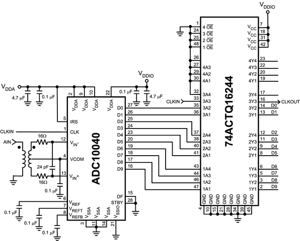
ADC10040CIMTX/NOPB 电路图
ADC10040CIMTX/NOPB 相关产品
- 100301QC
- 100304QC
- 100310QC
- 100311QC
- 100313QC
- 100316QC
- 100322QC
- 100329APC
- 100329DC
- 100336DC
- 100336PC
- 100341QC
- 100351DC
- 100351PC
- 100363QC
- 100364QC
- 100370QC
- 100390QC
- 100398QI
- 11AA010T-I/TT
- 11AA160T-I/TT
- 11LC010T-I/TT
- 11LC020T-I/TT
- 11LC040T-E/TT
- 11LC160T-E/TT
- 1ED020I12-F
- 2304NZGI-1LF
- 23A640-I/SN
- 23K256-I/SN
- 23K256-I/ST