 搜索
搜索
 发布采购
发布采购
ADC08D500CIYB/NOPB
数据转换 IC- 参考价格:¥1,257.25
更新日期:2024-04-01 00:04:00
ADC08D500CIYB/NOPB 供应商
- 公司
- 型号
- 品牌
- 封装/批号
- 数量
- 地区
- 日期
- 说明
- 询价
-
TI
-
原厂原装
22+ -
3288
-
上海市
-
-
-
一级代理原装
-
NS
-
128-eLQFP
22+授权代理 -
15800
-
上海市
-
-
-
旋尔只做进口原装,假一赔十...
-
TI
-
原厂原封装
新批号 -
887000
-
上海市
-
-
-
原厂发货进口原装微信同步QQ893727827
ADC08D500CIYB/NOPB 中文资料属性参数
- 制造商:National Semiconductor (TI)
- 转换器数量:2
- ADC 输入端数量:2
- 结构:2-Step Folding
- 转换速率:500000 KSPs
- 分辨率:8 bit
- 输入类型:Voltage
- 接口类型:Parallel
- 信噪比:48 dB
- 电压参考:Internal
- Supply Voltage - Max:2 V
- Supply Voltage - Min:1.8 V
- 最大功率耗散:2000 mW
- 最大工作温度:+ 85 C
- 安装风格:SMD/SMT
- 封装 / 箱体:LQFP EP
- 封装:Tray
- 最小工作温度:- 40 C
- 工作电源电压:1.9 V
- 工厂包装数量:60
产品特性
- Internal Sample-and-Hold
- Single +1.9V ±0.1V Operation
- Choice of SDR or DDR Output Clocking
- Interleave Mode for 2x Sampling Rate
- Multiple ADC Synchronization Capability
- Ensured No Missing Codes
- Serial Interface for Extended Control
- Fine Adjustment of Input Full-Scale Range and Offset
- Duty Cycle Corrected Sample Clock
- Resolution 8 Bits
- Max Conversion Rate 500 MSPS (min)
- Bit Error Rate 10-18 (typ)
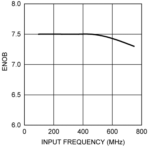
- ENOB @ 250 MHz Input 7.5 Bits (typ)
- DNL ±0.15 LSB (typ)
- Power ConsumptionOperating 1.4 W (typ)Power Down Mode 3.5 mW (typ)
- Operating 1.4 W (typ)
- Power Down Mode 3.5 mW (typ)
产品概述
The ADC08D500 is a dual, low power, high performance CMOS analog-to-digital converter
that digitizes signals to 8 bits resolution at sampling rates up to 500 MSPS. Consuming a typical
1.4 Watts at 500 MSPS from a single 1.9 Volt supply, this device is ensured to have no missing
codes over the full operating temperature range. The unique folding and interpolating architecture,
the fully differential comparator design, the innovative design of the internal sample-and-hold
amplifier and the self-calibration scheme enable a very flat response of all dynamic parameters
beyond Nyquist, producing a high 7.5 ENOB with a 250 MHz input signal and a 500 MHz sample rate
while providing a 10-18 B.E.R. Output formatting is offset binary and
the LVDS digital outputs are compatible with IEEE 1596.3-1996, with the exception of an adjustable
common mode voltage between 0.8V and 1.2V.Each converter has a 1:2 demultiplexer that feeds two LVDS buses and reduces the output
data rate on each bus to half the sampling rate. The two converters can be interleaved and used as
a single 1 GSPS ADC.The converter typically consumes less than 3.5 mW in the Power Down Mode and is available
in a 128-lead, thermally enhanced exposed pad HLQFP and operates over the Industrial (-40°C ≤
TA ≤ +85°C) temperature range.
ADC08D500CIYB/NOPB 电路图
ADC08D500CIYB/NOPB 电路图
ADC08D500CIYB/NOPB 相关产品
- 100301QC
- 100304QC
- 100310QC
- 100311QC
- 100313QC
- 100316QC
- 100322QC
- 100329APC
- 100329DC
- 100336DC
- 100336PC
- 100341QC
- 100351DC
- 100351PC
- 100363QC
- 100364QC
- 100370QC
- 100390QC
- 100398QI
- 11AA010T-I/TT
- 11AA160T-I/TT
- 11LC010T-I/TT
- 11LC020T-I/TT
- 11LC040T-E/TT
- 11LC160T-E/TT
- 1ED020I12-F
- 2304NZGI-1LF
- 23A640-I/SN
- 23K256-I/SN
- 23K256-I/ST