 搜索
搜索
 发布采购
发布采购
更新日期:2024-04-01 00:04:00

产品简介:耐辐射加固保障 (RHA)、QMLV、300krad、陶瓷、8 位、双通道 1.5GSPS 或单通道 3GSPS ADC
查看详情ADC08D1520WGFQV 供应商
- 公司
- 型号
- 品牌
- 封装/批号
- 数量
- 地区
- 日期
- 说明
- 询价
-
TI
-
N/A
22+授权代理 -
15800
-
上海市
-
-
-
旋尔只做进口原装,假一赔十...
-
TI
-
CFP-128
21+ -
2000
-
上海市
-
-
-
原装现货!品质为先!请来电垂询!
ADC08D1520WGFQV 中文资料属性参数
- 现有数量:0现货15Factory
- 价格:在售
- 系列:-
- 包装:托盘
- 产品状态:在售
- 位数:8
- 采样率(每秒):3G
- 输入数:2
- 输入类型:差分,单端
- 数据接口:LVDS - 并联,串行
- 配置:MUX-S/H-ADC
- 比率 - S/H:ADC:1:1
- A/D 转换器数:2
- 架构:折叠内插
- 参考类型:内部
- 电压 - 供电,模拟:1.8V ~ 2V
- 电压 - 供电,数字:1.8V ~ 2V
- 特性:-
- 工作温度:-55°C ~ 125°C(TA)
- 封装/外壳:128-TQFP
- 供应商器件封装:128-TQFP(14x14)
- 安装类型:表面贴装型
产品特性
- Total Ionizing Dose 300 krad(Si)
- Single Event Latch-up 120 MeV-cm2/mg
- Single +1.9V ±0.1V Operation
- Interleave Mode for 2x Sample Rate
- Multiple ADC Synchronization Capability
- Adjustment of Input Full-Scale Range, Offset and Clock Phase Adjustment
- Choice of SDR or DDR output clocking
- 1:1 or 1:2 Selectable Output Demux
- Second DCLK output
- Duty Cycle Corrected Sample Clock
- Test pattern
- Serial Interface for Extended Control
- Resolution 8 Bits
- Max Conversion Rate 1.5 GSPS (min)
- Code Error Rate 10-18 (typ)
- ENOB at 748 MHz Input 7.2 Bits (typ)
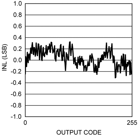
- DNL ±0.15 LSB (typ)
- Power ConsumptionOperating in 1:2 Demux Output 2.0 W (typ)Power Down Mode 2.9 mW (typ)
- Operating in 1:2 Demux Output 2.0 W (typ)
- Power Down Mode 2.9 mW (typ)
产品概述
The ADC08D1520 is an 8–Bit, dual channel, low power, high performance CMOS
analog-to-digital converter that builds upon the ADC08D1000 platform. The ADC08D1520 digitizes
signals to 8 bits of resolution at sample rates up to 1.7 GSPS. It has expanded features compared
to the ADC08D1000, which include a test pattern output for system debug, clock phase adjust, and
selectable output demultiplexer modes. Consuming a typical 2.0W in Demultiplex Mode at 1.5 GSPS
from a single 1.9 Volt supply, this device is ensured to have no missing codes over the full
operating temperature range. The unique folding and interpolating architecture, the fully
differential comparator design, the innovative design of the internal sample-and-hold amplifier and
the self-calibration scheme enable a very flat response of all dynamic parameters beyond Nyquist,
producing a high 7.2 Effective Number of Bits (ENOB) with a 748 MHz input signal and a 1.5 GHz
sample rate while providing a 10-18 Code Error Rate (C.E.R.) Output
formatting is offset binary and the Low Voltage Differential Signaling (LVDS) digital outputs are
compatible with IEEE 1596.3-1996, with the exception of an adjustable common mode voltage between
0.8V and 1.2V.Each converter has a selectable output demultiplexer which feeds two LVDS buses. If the
1:2 Demultiplexed Mode is selected, the output data rate is reduced to half the input sample rate
on each bus. When Non-Demultiplexed Mode is selected, the output data rate on channels DI and DQ
are at the same rate as the input sample clock. The two converters can be interleaved and used as a
single 3 GSPS ADC.The converter typically consumes less than 2.9 mW in the Power Down Mode and is available
in a 128-pin, thermally enhanced, multi-layer ceramic quad package and operates over the Military
(-55°C ≤ TA ≤ +125°C) temperature range.
ADC08D1520WGFQV 电路图
ADC08D1520WGFQV 电路图
ADC08D1520WGFQV 相关产品
- 5962-0720401VXC
- 5962-0720801VXC
- 5962-87802012A
- 5962-9152101MXA
- 5962-9961601HXA
- 6PA3100IRHBRQ1
- AD2S1210SST-EP-RL7
- AD2S1210WDSTZ
- AD2S80ATD/B
- AD3421QRWERQ1
- AD3421QRWETQ1
- AD5122ABCPZ100-RL7
- AD5122BCPZ100-RL7
- AD5122BRUZ10
- AD5123BCPZ100-RL7
- AD5142BCPZ10-RL7
- AD5235BRU25-EP-RL7
- AD5317RBRUZ
- AD5317RBRUZ-RL7
- AD5372BCPZ
- AD5623RBCPZ-5REEL7
- AD5628BCBZ-1-RL7
- AD5668BCPZ-1500RL7
- AD5684ARUZ
- AD5684BCPZ-RL7
- AD5684BRUZ-RL7
- AD5686ACPZ-RL7
- AD5686ARUZ
- AD5686BRUZ
- AD5686BRUZ-RL7