 搜索
搜索
 发布采购
发布采购
- 参考价格:¥3,291.65
更新日期:2024-04-01 00:04:00

产品简介:8 位、双路 1.0GSPS 或单路 2.0GSPS 模数转换器 (ADC)
查看详情- 参考价格:¥3,291.65
ADC08D1020CIYB 供应商
- 公司
- 型号
- 品牌
- 封装/批号
- 数量
- 地区
- 日期
- 说明
- 询价
-
NS
-
-
23+ -
5800
-
上海市
-
-
-
进口原装现货,杜绝假货。
-
National Semiconductor
-
HLQFP128
21+ -
47
-
上海市
-
-
-
一级代理原装
-
TI(德州仪器)
-
LQFP-128EP
2022+ -
12000
-
上海市
-
-
-
原装可开发票
-
TI
-
QFP
21+ -
268
-
上海市
-
-
-
原装现货,品质为先!请来电垂询!
-
ADI
-
PQFP
2112 -
70
-
台州
-
-
ADC08D1020CIYB 中文资料属性参数
- 制造商:National Semiconductor (TI)
- 转换器数量:2
- ADC 输入端数量:2
- 结构:2-Step Folding
- 转换速率:1000000 KSPs
- 分辨率:8 bit
- 输入类型:Voltage
- 接口类型:Parallel
- 信噪比:46.8 dB
- 电压参考:Internal
- Supply Voltage - Max:2 V
- Supply Voltage - Min:1.8 V
- 最大功率耗散:1600 mW
- 最大工作温度:+ 85 C
- 安装风格:SMD/SMT
- 封装 / 箱体:LQFP EP
- 封装:Tray
- 最小工作温度:- 40 C
- 工作电源电压:1.9 V
产品特性
- Single +1.9V ±0.1V Operation
- Interleave Mode for 2x Sample Rate
- Multiple ADC Synchronization Capability
- Adjustment of Input Full-Scale Range, Offset, and Clock Phase Adjust
- Choice of SDR or DDR Output Clocking
- 1:1 or 1:2 Selectable Output Demux
- Second DCLK Output
- Duty Cycle Corrected Sample Clock
- Test Pattern
- Resolution: 8 Bits
- Max Conversion Rate: 1 GSPS (min)
- Code Error Rate: 10−18 (typ)
- ENOB @ 498 MHz Input (Normal Mode): 7.4 Bits (typ)
- DNL: ±0.15 LSB (typ)
- Power ConsumptionOperating in Non-Demux Output: 1.6 W (typ)Operating in 1:2 Demux Output: 1.7 W (typ)Power Down Mode: 3.5 mW (typ)
- Operating in Non-Demux Output: 1.6 W (typ)
- Operating in 1:2 Demux Output: 1.7 W (typ)
- Power Down Mode: 3.5 mW (typ)
产品概述
The ADC08D1020 is a dual, low power, high performance, CMOS analog-to-digital converter
that builds upon the ADC08D1000 platform. The ADC08D1020 digitizes signals to 8 bits of resolution
at sample rates up to 1.3 GSPS. It has expanded features compared to the ADC08D1000, which include
a test pattern output for system debug, a clock phase adjust, and selectable output demultiplexer
modes. Consuming a typical 1.6 Watts in non-demultiplex mode at 1 GSPS from a single 1.9 Volt
supply, this device is ensured to have no missing codes over the full operating temperature range.
The unique folding and interpolating architecture, the fully differential comparator design, the
innovative design of the internal sample-and-hold amplifier and the calibration schemes enable a
very flat response of all dynamic parameters beyond Nyquist, producing a high 7.4 Effective Number
of Bits (ENOB) with a 498 MHz input signal and a 1 GHz sample rate while providing a
10−18 Code Error Rate (C.E.R.) Output formatting is offset binary and
the Low Voltage Differential Signaling (LVDS) digital outputs are compatible with IEEE 1596.3-1996,
with the exception of an adjustable common mode voltage between 0.8V and 1.2V.Each converter has a selectable output demultiplexer which feeds two LVDS buses. If the
1:2 demultiplexed mode is selected, the output data rate is reduced to half the input sample rate
on each bus. When non-demultiplexed mode is selected, that output data rate on channels DI and DQ
are at the same rate as the input sample clock. The two converters can be interleaved and used as a
single 2 GSPS ADC.The converter typically consumes less than 3.5 mW in the Power Down Mode and is available
in a leaded or lead-free 128-lead, thermally enhanced, exposed pad, HLQFP and operates over the
Industrial (-40°C ≤ TA ≤ +85°C) temperature range.
ADC08D1020CIYB 电路图
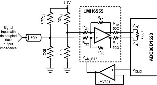
ADC08D1020CIYB 电路图
ADC08D1020CIYB 相关产品
- 100301QC
- 100304QC
- 100310QC
- 100311QC
- 100313QC
- 100316QC
- 100322QC
- 100329APC
- 100329DC
- 100336DC
- 100336PC
- 100341QC
- 100351DC
- 100351PC
- 100363QC
- 100364QC
- 100370QC
- 100390QC
- 100398QI
- 11AA010T-I/TT
- 11AA160T-I/TT
- 11LC010T-I/TT
- 11LC020T-I/TT
- 11LC040T-E/TT
- 11LC160T-E/TT
- 1ED020I12-F
- 2304NZGI-1LF
- 23A640-I/SN
- 23K256-I/SN
- 23K256-I/ST