 搜索
搜索
 发布采购
发布采购
- 参考价格:¥156.63-¥164.98
更新日期:2024-04-01 00:04:00

产品简介:缓冲区容量为 1K 的 8 位、200MSPS 模数转换器 (ADC)
查看详情- 参考价格:¥156.63-¥164.98
ADC08B200CIVS 供应商
- 公司
- 型号
- 品牌
- 封装/批号
- 数量
- 地区
- 日期
- 说明
- 询价
-
TI
-
原厂原装
22+ -
3288
-
上海市
-
-
-
一级代理原装
-
NS
-
-
7 -
500
-
杭州
-
-
-
原装正品现货
-
TI/NS
-
-
21+ -
5000
-
上海市
-
-
-
原装现货,品质为先!请来电垂询!
ADC08B200CIVS 中文资料属性参数
- 制造商:National Semiconductor (TI)
- 转换器数量:1
- ADC 输入端数量:1
- 转换速率:200000 KSPs
- 分辨率:8 bit
- 输入类型:Voltage
- 接口类型:Parallel
- 信噪比:47 dB
- 电压参考:External
- Supply Voltage - Max:3.6 V
- Supply Voltage - Min:3 V
- 最大工作温度:+ 105 C
- 安装风格:SMD/SMT
- 封装 / 箱体:TQFP-48
- 封装:Tray
- 最小工作温度:- 40 C
- 工作电源电压:3.3 V
- 工厂包装数量:250
产品特性
- Single-Ended Input
- Selectable Capture Buffer Size
- PLL for Clock Multiplication
- Reference Ladder Top and Bottom Accessible
- Linear Power Scaling with Sample Rate
- FPGA Training Pattern
- AEC-Q100 Grade 2 Qualified
- Power-Down Feature
- Resolution 8 Bits
- Maximum Sampling Frequency 200 MSPS (min)
- DNL ±0.4 LSB (typ)
- ENOB (fIN= 49 MHz) 7.2 bits (typ)
- THD (fIN= 49 MHz) −53 dBc (typ)
- Power ConsumptionOperating (50 MHz) Input 2 mW / Msps (typ)Power Down 2.15 mW (typ)
- Operating (50 MHz) Input 2 mW / Msps (typ)
- Power Down 2.15 mW (typ)
产品概述
The ADC08B200 is a high speed analog-to-digital converter (ADC) with an integrated
capture buffer. The 8-bit, 200 MSPS A/D core is based upon the proven ADC08200 with integrated
track-and-hold and is optimized for low power consumption. This device contains a selectable size
capture buffer of up to 1,024 bytes that allows fast capture of an input signal with a slower
readout rate. An on-chip clock PLL circuit provides the option of on-chip clock rate multiplication
to provide the high speed sampling clock.The ADC08B200 is resistant to latch-up and the outputs are short-circuit proof. The top
and bottom of the ADC08B200's reference ladder are available for connections, enabling a wide range
of input possibilities. The digital outputs are TTL/CMOS compatible with a separate output power
supply pin to support interfacing with 2.7V to 3.3V logic. The digital inputs and outputs are low
voltage TTL/CMOS compatible and the output data format is straight binary.The ADC08B200Q runs on an Automotive Grade Flow and is AEC-Q100 Grade 2 Qualified.The ADC08B200 is offered in a 48-pin plastic package (TQFP) and is specified over the
extended industrial temperature range of −40°C to +105°C. An evaluation board is available to
assist in the easy evaluation of the ADC08B200.
ADC08B200CIVS 数据手册
| 数据手册 | 说明 | 数量 | 操作 |
|---|---|---|---|
 ADC08B200CIVS/NOPB ADC08B200CIVS/NOPB
|
8 Bit Analog to Digital Converter 1 Input 48-TQFP (7x7) |
39页,824K | 查看 |
ADC08B200CIVS 电路图
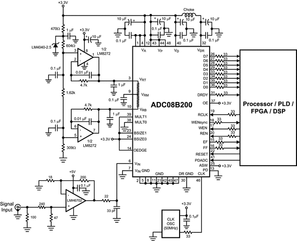
ADC08B200CIVS 电路图
ADC08B200CIVS 相关产品
- 100301QC
- 100304QC
- 100310QC
- 100311QC
- 100313QC
- 100316QC
- 100322QC
- 100329APC
- 100329DC
- 100336DC
- 100336PC
- 100341QC
- 100351DC
- 100351PC
- 100363QC
- 100364QC
- 100370QC
- 100390QC
- 100398QI
- 11AA010T-I/TT
- 11AA160T-I/TT
- 11LC010T-I/TT
- 11LC020T-I/TT
- 11LC040T-E/TT
- 11LC160T-E/TT
- 1ED020I12-F
- 2304NZGI-1LF
- 23A640-I/SN
- 23K256-I/SN
- 23K256-I/ST