 搜索
搜索
 发布采购
发布采购
更新日期:2024-04-01 00:04:00

产品简介:8 位并行输出串行移位寄存器
查看详情84162012A 供应商
- 公司
- 型号
- 品牌
- 封装/批号
- 数量
- 地区
- 日期
- 说明
- 询价
-
Texas Instruments
-
LCCC20
21+ -
21
-
上海市
-
-
-
一级代理原装
84162012A 中文资料属性参数
- 现有数量:0现货2,539Factory
- 价格:在售
- 系列:*
- 包装:管件
- 产品状态:在售
- 逻辑类型:-
- 输出类型:-
- 元件数:-
- 每个元件位数:-
- 功能:-
- 电压 - 供电:-
- 工作温度:-
- 安装类型:-
- 封装/外壳:-
- 供应商器件封装:-
产品特性
- Wide Operating Voltage Range of 2 V to 6 V
- Outputs Can Drive Up to 10 LSTTL Loads
- Low Power Consumption, 80-µA Maximum ICC
- Typical tpd = 20 ns
- ±4-mA Output Drive at 5 V
- Low Input Current of 1-µA Maximum
- AND-Gated (Enable/Disable) Serial Inputs
- Fully Buffered Clock and Serial Inputs
- Direct Clear
- On Products Compliant to MIL-PRF-38535, All Parameters Are Tested Unless Otherwise Noted. On All Other Products, Production Processing Does Not Necessarily Include Testing of All Parameters.
产品概述
These 8-bit shift registers feature AND-gated serial inputs and an asynchronous clear
(CLR) input. The gated serial (A and B) inputs permit complete control over
incoming data; a low at either input inhibits entry of the new data and resets the first flip-flop
to the low level at the next clock (CLK) pulse. A high-level input enables the other input, which
then determines the state of the first flip-flop. Data at the serial inputs can be changed while
CLK is high or low, provided the minimum set-up time requirements are met. Clocking occurs on the
low-to-high-level transition of CLK.
84162012A 电路图
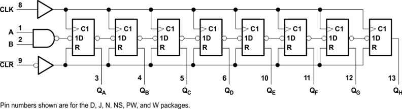
84162012A 电路图
84162012A 相关产品
- 1P1G125QDRYRQ1
- 1P1G126QDRYRQ1
- 1P2GU04QDRYRQ1
- 2N7001TDCKR
- 2N7001TDPWR
- 54FCT245TDB
- 5962-8762401CA
- 5962-8766301MRA
- 5962-8768001EA
- 7202LA50JG
- 7203L20TDB
- 7204L35J
- 72805LB15PF
- 7280L20PA
- 72V201L15PFGI
- 72V211L10PFG
- 72V245L10PFG
- 72V3640L10PF
- 72V3660L7-5PFI
- 72V70210DAG
- 72V70840DAG
- 72V73273BBG
- 74AHC05S14-13
- 74AHC05T14-13
- 74AHC1G126MDCKTEP
- 74AHC32S14-13
- 74AHC594S16-13
- 74AHC594T16-13
- 74AHCT08PW-Q100J
- 74AHCT125S14-13