 搜索
搜索
 发布采购
发布采购
- 参考价格:¥1.01-¥2.90
更新日期:2024-04-01 00:04:00

74LVC2G125DCTRG4 供应商
- 公司
- 型号
- 品牌
- 封装/批号
- 数量
- 地区
- 日期
- 说明
- 询价
-
TI
-
原厂原装
22+ -
3288
-
上海市
-
-
-
一级代理原装
-
TI(德州仪器)
-
SM8(SSOP)
2022+ -
12000
-
上海市
-
-
-
原装可开发票
74LVC2G125DCTRG4 中文资料属性参数
- 制造商:Texas Instruments
- 产品种类:缓冲器和线路驱动器
- 输入线路数量:2
- 输出线路数量:2
- 极性:Non-Inverting
- Supply Voltage - Max:5.5 V
- Supply Voltage - Min:1.65 V
- 最大工作温度:+ 85 C
- 安装风格:SMD/SMT
- 封装 / 箱体:SSOP-8
- 封装:Reel
- 高电平输出电流:- 32 mA
- 逻辑系列:LVC
- 逻辑类型:CMOS
- 低电平输出电流:32 mA
- 最小工作温度:- 40 C
- 每芯片的通道数量:2
- 输出类型:3-State
- 传播延迟时间:4.3 ns at 3.3 V, 3.7 ns at 5 V
- 工厂包装数量:3000
产品特性
- ESD Protection Exceeds JESD 22 2000-V Human-Body Model 1000-V Charged-Device Model
- 2000-V Human-Body Model
- 1000-V Charged-Device Model
- Available in the Texas Instruments NanoFree™ Package
- Supports 5-V VCC Operation
- Inputs Accept Voltages to 5.5 V
- Max tpd of 4.3 ns at 3.3 V
- Low Power Consumption, 10-µA Max ICC
- ±24-mA Output Drive at 3.3 V
- Typical VOLP (Output Ground Bounce) < 0.8 V at VCC = 3.3 V, TA = 25°C
- Typical VOHV (Output VOH Undershoot) > 2 V at VCC = 3.3 V, TA = 25°C
- Ioff Supports Live Insertion, Partial-Power-Down Mode, and Back-Drive Protection
- Can Be Used as a Down Translator to Translate Inputs From a Max of 5.5 V Down to the VCC Level
- Latch-Up Performance Exceeds 100 mA Per JESD 78, Class II
产品概述
The SN74LVC2G125 device is a dual bus buffer gate, designed for 1.65-V to 5.5-V
VCC operation. This device features dual line drivers with 3-state outputs.
The outputs are disabled when the associated output-enable (OE) input is
high.NanoFree™ package technology is a major breakthrough in IC packaging concepts, using the
die as the package.To ensure the high-impedance state during power up or power down,
OE should be tied to VCC through a pullup resistor;
the minimum value of the resistor is determined by the current-sinking capability of the
driver.This device is fully specified for partial-power-down applications using
Ioff. The Ioff circuitry disables the outputs,
preventing damaging current backflow through the device when it is powered down.
74LVC2G125DCTRG4 电路图
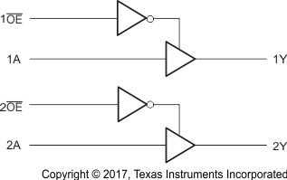
74LVC2G125DCTRG4 电路图
74LVC2G125DCTRG4 相关产品
- 100301QC
- 100304QC
- 100310QC
- 100311QC
- 100313QC
- 100316QC
- 100322QC
- 100329APC
- 100329DC
- 100336DC
- 100336PC
- 100341QC
- 100351DC
- 100351PC
- 100363QC
- 100364QC
- 100370QC
- 100390QC
- 100398QI
- 11AA010T-I/TT
- 11AA160T-I/TT
- 11LC010T-I/TT
- 11LC020T-I/TT
- 11LC040T-E/TT
- 11LC160T-E/TT
- 1ED020I12-F
- 2304NZGI-1LF
- 23A640-I/SN
- 23K256-I/SN
- 23K256-I/ST