 搜索
搜索
 发布采购
发布采购
HEF4013BT
触发器- 参考价格:CNY 0.772-CNY 3.05
更新日期:2024-04-01 00:04:00
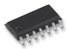
HEF4013BT
触发器- 参考价格:CNY 0.772-CNY 3.05
HEF4013BT 供应商
- 公司
- 型号
- 品牌
- 封装/批号
- 数量
- 地区
- 日期
- 说明
- 询价
-
NXP/恩智浦
-
SOP14
24+ -
1000
-
深圳
-
-
-
只做原装,好价支持
-
NXP
-
SOP-14
- -
2292
-
上海市
-
-
-
经营22年实体店原装,具体年份和数量以实际为准
-
NXP/PHI
-
SOP
10+ -
100000
-
杭州
-
-
-
原装正品现货
-
NXP/恩智浦
-
SMD
21+ -
10000
-
杭州
-
-
-
只做原装现货,大量现货热卖
-
-
2019+ -
5800
-
上海市
-
-
-
全新原装现货
-
NXP
-
SOP14
22+授权代理 -
15800
-
上海市
-
-
-
旋尔只做进口原装,假一赔十...
-
Philips
-
TSOP
23+ -
15000
-
上海市
-
-
-
中国区代理原装现货热卖特价
-
NXP/PHI
-
SOP
21+ -
2000
-
上海市
-
-
-
原装现货,品质为先!请来电垂询!
-
NXP
-
原装进口
15+ -
600000
-
上海市
-
-
-
原装进口现货,价格优势,开增值税17发票。
-
NXP
-
SOP-14
23+ -
5800
-
上海市
-
-
-
进口原装现货,杜绝假货。
HEF4013BT 中文资料属性参数
- 触发类型::D
- 传播延迟??间::30ns
- 频率::40MHz
- 输出电流::2.4mA
- 触发类型::上升沿
- 输出类型::互补
- 电源电压范围::4.5V 到 15.5V
- 封装类型::SOIC
- 针脚数::14
- 工作温度范围::-40°C 到 +70°C
- SVHC(高度关注物质)::No SVHC (18-Jun-2012)
- 器件标号::4013
- 器件标记::HEF4013BT
- 封装类型::SOIC
- 工作温度敏::-40°C
- 工作温度最高::70°C
- 电源电压::15V
- 电源电压 最大::15V
- 电源电压 最小::3V
- 芯片标号::4013
- 表面安装器件::表面安装
- 输入数::1
- 输出类型::差分
- 逻辑功能号::4013
- 逻辑芯片功能::双D触发器
- 逻辑芯片基本号::4013
- 逻辑芯片系列::4000 CMOS
- 门电路数::2
HEF4013BT 数据手册
| 数据手册 | 说明 | 数量 | 操作 |
|---|---|---|---|
 HEF4013BT HEF4013BT
|
Dual D-type flip-flop |
7 Pages页,80K | 查看 |
|
HEF4013BT
|
1. General description The HEF4013B is a dual D-type flip-flop that features independent set-direct input (SD), clear-direct input (CD), clock input (CP) and outputs (Q, Q). Data is accepted when CP is LOW and is transferred to the output on the positive-going edge of the clock. The active HIGH asynchronous CD and SD inputs are independent and override the D or CP inputs. The outputs are buffered for best system performance. The clock input’s Schmitt-trigger action makes the circuit highly tolerant of slower clock rise and fall times. It operates over a recommended V DD power supply range of 3 V to 15 V referenced to V SS (usually ground). Unused inputs must be connected to V DD , V SS , or another input. 2. Features and benefits ? Tolerant of slow clock rise and fall times ? Fully static operation ? 5 V, 10 V, and 15 V parametric ratings ? Standardized symmetrical output characteristics ? Specified from ?40 ?C to +125 ?C ? Complies with JEDEC standard JESD 13-B 3. Applications |
17页,127K | 查看 |
|
HEF4013BT
|
DATA SHEET Product speci?cation File under Integrated Circuits, IC04 January 1995 INTEGRATED CIRCUITS HEF4013B flip-flops Dual D-type flip-flop For a complete data sheet, please also download: ? The IC04 LOCMOS HE4000B Logic Family Specifications HEF, HEC ? The IC04 LOCMOS HE4000B Logic Package Outlines/Information HEF, HEC |
7页,84K | 查看 |
|
HEF4013BT_1272
|
1. General description The HEF4013B is a dual D-type flip-flop that features independent set-direct input (SD), clear-direct input (CD), clock input (CP) and outputs (Q, Q). Data is accepted when CP is LOW and is transferred to the output on the positive-going edge of the clock. The active HIGH asynchronous CD and SD inputs are independent and override the D or CP inputs. The outputs are buffered for best system performance. The clock input’s Schmitt-trigger action makes the circuit highly tolerant of slower clock rise and fall times. It operates over a recommended V DD power supply range of 3 V to 15 V referenced to V SS (usually ground). Unused inputs must be connected to V DD , V SS , or another input. 2. Features and benefits ? Tolerant of slow clock rise and fall times ? Fully static operation ? 5 V, 10 V, and 15 V parametric ratings ? Standardized symmetrical output characteristics ? Specified from ?40 ?C to +125 ?C ? Complies with JEDEC standard JESD 13-B 3. Applications |
17页,127K | 查看 |
|
HEF4013BTD
|
Dual D-type flip-flop |
7 Pages页,80K | 查看 |