 搜索
搜索
 发布采购
发布采购
- 参考价格:¥14.70
更新日期:2024-04-01 00:04:00

DS90C385AMTX 供应商
- 公司
- 型号
- 品牌
- 封装/批号
- 数量
- 地区
- 日期
- 说明
- 询价
-
TI
-
原厂原装
22+ -
3288
-
上海市
-
-
-
一级代理原装
-
TI
-
-
21+ -
12500
-
上海市
-
-
-
原装现货,品质为先,请来电垂询!
-
NS
-
TSSOP56
新批号 -
8877000
-
上海市
-
-
-
原厂发货进口原装微信同步QQ893727827
-
TI
-
TSSOP56
22+ -
300000
-
常州
-
-
-
原装正品
-
NS
-
TSSOP56
23+ -
5800
-
上海市
-
-
-
进口原装现货,杜绝假货。
-
-
23+ -
46000
-
合肥
-
-
-
科大讯飞战略投资企业,提供一站式配套服务
-
TI/德州仪器
-
TSSOP-56
24+ -
10000
-
上海市
-
-
-
上海现货
-
TI/德州仪器
-
TSSOP56
21+ -
10000
-
杭州
-
-
-
只做原装现货,大量现货热卖
-
TI(德州仪器)
-
TSSOP-56
2022+ -
6187
-
上海市
-
-
-
原装可开发票
-
NS/ELNAF
-
TSSOP-5
1805+ -
12403
-
上海市
-
-
-
原装现货,精专配套,正品BOM表报价
DS90C385AMTX 中文资料属性参数
- 制造商:National Semiconductor (TI)
- 激励器数量:4
- 接收机数量:28
- 数据速率:2450 Mbps
- 工作电源电压:3.3 V
- 最大功率耗散:1630 mW
- 最大工作温度:+ 70 C
- 封装 / 箱体:TSSOP-56
- 封装:Reel
- 最小工作温度:- 10 C
- 安装风格:SMD/SMT
- 工厂包装数量:1000
- Supply Voltage - Max:3.6 V
- Supply Voltage - Min:3 V
- 类型:LVDS
产品特性
- Pin-to-Pin Compatible to DS90C383, DS90C383A and DS90C385
- No Special Start-Up Sequence Required between Clock/Data and /PD Pins. Input Signals (Clock and Data) can be Applied Either Before or After the Device is Powered.
- Support Spread Spectrum Clocking up to 100kHz Frequency Modulation and Deviations of ±2.5% Center Spread or -5% Down Spread
- “Input Clock Detection" Feature Will Pull All LVDS Pairs to Logic Low When Input Clock is Missing and When /PD Pin is Logic High
- 18 to 87.5 MHz Shift Clock Support
- Tx Power Consumption < 147 mW (typ) at 87.5MHz Grayscale
- Tx Power-Down Mode < 60 μW (typ)
- Supports VGA, SVGA, XGA, SXGA(Dual Pixel), SXGA+(Dual Pixel), UXGA(Dual Pixel).
- Narrow Bus Reduces Cable Size and Cost
- Up to 2.45 Gbps Throughput
- Up to 306.25Megabyte/sec Bandwidth
- 345 mV (typ) Swing LVDS Devices for Low EMI
- PLL Requires No External Components
- Compliant to TIA/EIA-644 LVDS standard
- Low Profile 56-lead TSSOP Package
产品概述
The DS90C385A is a pin to pin compatible replacement for DS90C383, DS90C383A and
DS90C385. The DS90C385A has additional features and improvements making it an ideal replacement for
DS90C383, DS90C383A and DS90C385. family of LVDS Transmitters.The DS90C385A transmitter converts 28 bits of LVCMOS/LVTTL data into four LVDS (Low
Voltage Differential Signaling) data streams. A phase-locked transmit clock is transmitted in
parallel with the data streams over the fifth LVDS link. Every cycle of the transmit clock 28 bits
of input data are sampled and transmitted. At a transmit clock frequency of 87.5 MHz, 24 bits of
RGB data and 3 bits of LCD timing and control data (FPLINE, FPFRAME, DRDY) are transmitted at a
rate of 612.5Mbps per LVDS data channel. Using a 87.5 MHz clock, the data throughput is
306.25Mbytes/sec. This transmitter can be programmed for Rising edge strobe or Falling edge strobe
through a dedicated pin. A Rising edge or Falling edge strobe transmitter will interoperate with a
Falling edge strobe FPDLink Receiver without any translation logic.This chipset is an ideal means to solve EMI and cable size problems associated with wide,
high-speed TTL interfaces with added Spread Spectrum Clocking support.
DS90C385AMTX 电路图
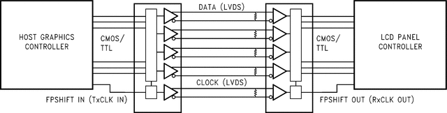
DS90C385AMTX 电路图
DS90C385AMTX 相关产品
- 100301QC
- 100304QC
- 100310QC
- 100311QC
- 100313QC
- 100316QC
- 100322QC
- 100329APC
- 100329DC
- 100336DC
- 100336PC
- 100341QC
- 100351DC
- 100351PC
- 100363QC
- 100364QC
- 100370QC
- 100390QC
- 100398QI
- 11AA010T-I/TT
- 11AA160T-I/TT
- 11LC010T-I/TT
- 11LC020T-I/TT
- 11LC040T-E/TT
- 11LC160T-E/TT
- 1ED020I12-F
- 2304NZGI-1LF
- 23A640-I/SN
- 23K256-I/SN
- 23K256-I/ST