 搜索
搜索
 发布采购
发布采购
- 参考价格:¥15.80
更新日期:2024-04-01 00:04:00

产品简介:+3.3V 可编程 LVDS 发送器 24 位平板显示 (FPD) 链接 - 65MHz
查看详情- 参考价格:¥15.80
DS90C383BMTX 供应商
- 公司
- 型号
- 品牌
- 封装/批号
- 数量
- 地区
- 日期
- 说明
- 询价
-
NS
-
-
7 -
500
-
杭州
-
-
-
原装正品现货
-
TI/NS
-
-
21+ -
5000
-
上海市
-
-
-
原装现货,品质为先,请来电垂询!
-
TI
-
TSSOP
23+ -
46000
-
合肥
-
-
-
科大讯飞战略投资企业,提供一站式配套服务
-
TI
-
原厂原装
22+ -
3288
-
上海市
-
-
-
一级代理原装
-
NSTI/ELNAF
-
TSSOP-5
1806+ -
3700
-
上海市
-
-
-
原装现货,精专配套,正品BOM表报价
-
TI(德州仪器)
-
TSSOP-56
2022+ -
12000
-
上海市
-
-
-
原装可开发票
DS90C383BMTX 中文资料属性参数
- 制造商:National Semiconductor (TI)
- 激励器数量:4
- 接收机数量:28
- 数据速率:455 Mbps
- 工作电源电压:3.3 V
- 最大功率耗散:1630 mW
- 最大工作温度:+ 70 C
- 封装 / 箱体:TSSOP-56
- 封装:Reel
- 最小工作温度:- 10 C
- 安装风格:SMD/SMT
- Supply Voltage - Max:3.6 V
- Supply Voltage - Min:3 V
- 类型:LVDS
产品特性
- No special start-up sequence required between clock/data and /PD pins. Input signal (clock and data) can be applied either before or after the device is powered
- Support Spread Spectrum Clocking up to 100kHz frequency modulation and deviations of ±2.5% center spread or -5% down spread
- "Input Clock Detection" feature will pull all LVDS pairs to logic low when input clock is missing and when /PD pin is logic high
- 18 to 68 MHz shift clock support
- Best-in-Class Setup and Hold Times on TxINPUTs
- Tx power consumption < 130 mW (typ) at 65MHz Grayscale
- 40% Less Power Dissipation than BiCMOS Alternatives
- Tx Power-down mode < 60μW (typ)
- Supports VGA, SVGA, XGA and Dual Pixel SXGA.
- Narrow bus reduces cable size and cost
- Up to 1.8 Gbps throughput
- Up to 227 Megabytes/sec bandwidth
- 345 mV (typ) swing LVDS devices for low EMI
- PLL requires no external components
- Compatible with TIA/EIA-644 LVDS standard
- Low profile 56-lead TSSOP package
- Improved replacement for: SN75LVDS83, DS90C383A
- SN75LVDS83, DS90C383A
产品概述
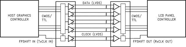
The DS90C383B transmitter converts 28 bits of CMOS/TTL data into four LVDS (Low Voltage
Differential Signaling) data streams. A phase-locked transmit clock is transmitted in parallel with
the data streams over a fifth LVDS link. Every cycle of the transmit clock 28 bits of input data
are sampled and transmitted. At a transmit clock frequency of 65 MHz, 24 bits of RGB data and 3
bits of LCD timing and control data (FPLINE, FPFRAME, DRDY) are transmitted at a rate of 455 Mbps
per LVDS data channel. Using a 65 MHz clock, the data throughput is 227 Mbytes/sec. The DS90C383B
transmitter can be programmed for Rising edge strobe or Falling edge strobe through a dedicated
pin. A Rising edge or Falling edge strobe transmitter will interoperate with a Falling edge strobe
Receiver (DS90CF386) without any translation logic.This chipset is an ideal means to solve EMI and cable size problems associated with wide,
high speed TTL interfaces.
DS90C383BMTX 数据手册
| 数据手册 | 说明 | 数量 | 操作 |
|---|---|---|---|
 DS90C383BMTX/NOPB DS90C383BMTX/NOPB
|
5/0 Driver FPD-Link, LVDS 56-TSSOP |
17页,1.24M | 查看 |
DS90C383BMTX 电路图
DS90C383BMTX 电路图
DS90C383BMTX 相关产品
- 100301QC
- 100304QC
- 100310QC
- 100311QC
- 100313QC
- 100316QC
- 100322QC
- 100329APC
- 100329DC
- 100336DC
- 100336PC
- 100341QC
- 100351DC
- 100351PC
- 100363QC
- 100364QC
- 100370QC
- 100390QC
- 100398QI
- 11AA010T-I/TT
- 11AA160T-I/TT
- 11LC010T-I/TT
- 11LC020T-I/TT
- 11LC040T-E/TT
- 11LC160T-E/TT
- 1ED020I12-F
- 2304NZGI-1LF
- 23A640-I/SN
- 23K256-I/SN
- 23K256-I/ST